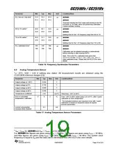
CC2510Fx / CC2511Fx
Parameter
Min
Typ
Max
Unit
Condition/Note
PLL turn-on / hop time4
72.4
81.4
75.2
81.4
81.4
81.4
µs
CC2510Fx
CC2511Fx
Time from leaving the IDLE state until arriving in the RX,
FSTXON, or TX state, when not performing calibration.
Crystal oscillator running.
RX to TX switch 4
TX to RX switch 4
PLL calibration time4
29.0
32.6
30.1
32.6
32.6
32.6
µs
µs
µs
CC2510Fx
CC2511Fx
Settling time for the 1·IF frequency step from RX to TX
30.0
33.6
31.1
33.6
33.6
33.6
CC2510Fx
CC2511Fx
Settling time for the 1·IF frequency step from TX to RX
707
796
735
796
796
796
CC2510Fx
CC2511Fx
Calibration can be initiated manually or automatically
before entering or after leaving RX/TX.
Note: This is the PLL calibration time given that
TEST0=0x0Band FSCAL3.CHP_CURR_CAL_EN=10
(max calibration time). Please see DN110 [11] for more
details
Table 16: Frequency Synthesizer Parameters
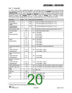
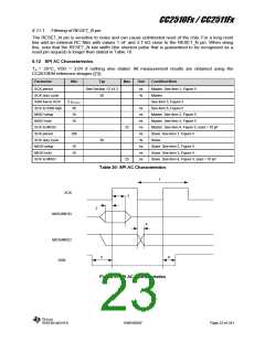
6.9 Analog Temperature Sensor
TA= 25°C, VDD = 3.0V if nothing else stated. All measurement results are obtained using the
CC2510EM reference designs ([1]).
Parameter
Min
Typ
Max
Unit
Condition/Note
0.654
0.750
0.848
0.946
2.43
0
V
V
V
V
Output voltage at −40°C
Output voltage at 0°C
Output voltage at 40°C
Output voltage at 80°C
Temperature coefficient
mV/°C Fitted from −20°C to 80°C
Error in calculated
temperature, calibrated
−2 *
2 *
°C
From −20°C to 80°C when using 2.43 mV/°C, after 1-point
calibration at room temperature
* The indicated minimum and maximum error with 1-point
calibration is based on measured values for typical
process parameters
Current consumption
0.3
mA
increase when enabled
Table 17: Analog Temperature Sensor Parameters
4 fRef = fXOSC for CC2510Fx and fRef = f fXOSC xosc/2 for CC2511Fx
For CC2510Fx Min figures are given using fXOSC = 27 MHz. Typ figures are given using fXOSC = 26 MHz,
and Max figures are given using fXOSC = 24 MHz. For CC2511Fx, fXOSC = 48 MHz The system clock
frequency is equal to fRef and the data rate is 250 kBaud. See DN110 [11] for more details.
SWRS055F
Page 19 of 241

 TI [ TEXAS INSTRUMENTS ]