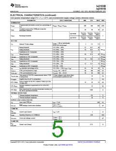
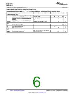
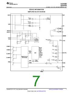
bq51050B
bq51051B
www.ti.com
SLUSB42C –JULY 2012–REVISED FEBRUARY 2013
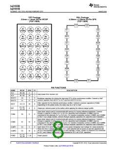
PIN FUNCTIONS (continued)
NAME
WCSP
QFN
I/O
DESCRIPTION
Programming pin for the battery charge current. Connect external resistor to VSS. Size RILIM with
the following equation: RILIM = 300 / IILIM where IILIM is the desired battery charge current.
ILIM
G1
12
I/O
Connect this pin to the wired adapter input. When a voltage is applied to this pin wireless charging is
disabled and AD_EN is driven low. Connect to GND through a 1µF capacitor. If unused, capacitor is
not required and should be grounded directly.
AD
G4
F3
F1
9
8
I
O
I
AD-EN
TS/CTRL
Push-pull driver for external PFET when wired charging is active.
Must be connected to ground via a NTC resistor. If an NTC function is not desired, connect to GND
with a 10 kΩ resistor. As a CTRL pin pull to ground to send end power transfer (EPT) fault to the
transmitter or pull-up to an internal rail (i.e. 1.8 V) to send EPT termination to the transmitter.
13
Input that allows the termination threshold to be programmable. KTERM = 240 Ω/%. Set the
termination threshold by applying the following equation RTERM = %IILIM × KTERM where %IILIM is the
desired percentage of fast charge current when termination should occur.
TERM
EN2
G3
G2
10
11
I
I
EN2=0 enables wired charging source if AD input volatge is above 3.6V, wireless charging is
enabled if AD input volatge is < 3.6V, EN2=1 disables wired charging source; wireless power is
always enabled if present.
FOD
CHG
F2
F4
14
7
I
Input for the rectified power measurement. Connect to GND with a 188 Ω resistor.
O
Open-drain output – active when charging of the battery is active.
Copyright © 2012–2013, Texas Instruments Incorporated
Submit Documentation Feedback
9
Product Folder Links: bq51050B bq51051B

 TI [ TEXAS INSTRUMENTS ]