bq51050B
bq51051B
www.ti.com
SLUSB42C –JULY 2012–REVISED FEBRUARY 2013
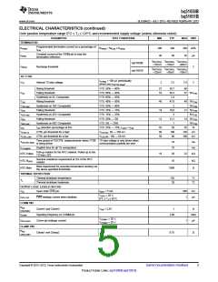
ELECTRICAL CHARACTERISTICS (continued)
Over junction temperature range 0°C ≤ TJ ≤ 125°C and recommended supply voltage (unless otherwise noted)
PARAMETER
TEST CONDITIONS
MIN
TYP
MAX UNIT
TERMINATION
Programmable termination current as a percentage of
IILIM
KTERM
ITERM
RTERM = %IILIM x KTERM
200
40
240
50
280
55
Ω/%
Constant current at the TERM pin to bias the
termination reference
µA
VBAT(REG) VBAT(REG) VBAT(REG)
–135mV –110mV –90mV
VBAT(REG) VBAT(REG) VBAT(REG)
bq51050B
bq51051B
VRECH
Recharge threshold
V
V
–125mV
–95mV
–70mV
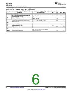
TS / CTRL
ITS-Bias < 100 µA (periodically
VTS
Internal TS bias voltage
2
2.2
2.4
60
driven see tTS/CTRL-Meas
VTS: 50% → 60%
VTS: 60% → 50%
VTS: 60% → 50%
VTS: 40% → 50%
VTS: 50% → 40%
VTS: 25% → 15%
VTS: 15% → 25%
VTS: 20% → 5%
VTS: 5% → 20%
)
Rising threshold
57
55
58.7
56.3
2.4
47.8
2
VOC
Falling threshold
57 %VTSB
Hysteresis on 0C Comparator
Rising threshold
V10C
46
18
12
49 %VTSB
%VTSB
V10C-Hyst
V45C
V45C-Hyst
V60C
V60C-Hyst
I45C
VCTRL-HI
VCTRL-LOW
Hysteresis on 10C Comparator
Falling threshold
19.6
3
21 %VTSB
%VTSB
Hysteresis on 45C Comparator
Falling threshold
13.1
1
14 %VTSB
%VTSB
Hysteresis on 60C Comparator
ILIM reduction percentage at 45c
CTRL pin threshold for a high
CTRL pin threshold for a low
VTS: 25% → 15%, ILOAD = IILIM
VTS/CTRL: 50 → 150 mV
45
80
50
50
55
130
100
%
100
80
mV
mV
VTS/CTRL: 150 → 50 mV
Time period of TS/CTRL measurements--when VTSB TS bias voltage is only driven when
TTS/CTRL-Meas
24
10
20
ms
ms
kΩ
is being driven
communication packets are sent
tTS-Deglitch
Deglitch time for all TS comparators
Pull-up resistor for the NTC network. Pulled up to the
TS bias LDO.
NTC-Pullup
18
22
Nominal resistance requirement at 25c of the NTC
resistor
NTC-RNOM
NTC-Beta
10
kΩ
Beta requirement for accurate temperature sensing via
the above specified thresholds
3380
Ω
THERMAL PROTECTION
Thermal shutdown temperature
Thermal shutdown hysteresis
OUTPUT LOGIC LEVELS ON /CHG
155
20
°C
°C
TJ
VOL
Open drain CHG pin
ISINK = 5 mA
500
1
mV
µA
VCHG = 20 V,
0°C ≤ TJ ≤ 85°C
IOFF,CHG
CHG leakage current when disabled
COMM PIN
RDS-
Comm1 and Comm2
Vrect = 2.6V
1
Ω
ON(COMM)
fCOMM
Signaling frequency on COMM pin
Comm pin leakage current
2.00
Kb/s
µA
VCOMM1 = 20 V,
VCOMM2 = 20 V
IOFF,Comm
1
CLAMP PIN
RDS-
Clamp1 and Clamp2
0.75
Ω
ON(CLAMP)
Copyright © 2012–2013, Texas Instruments Incorporated
Submit Documentation Feedback
5
Product Folder Links: bq51050B bq51051B

 TI [ TEXAS INSTRUMENTS ]