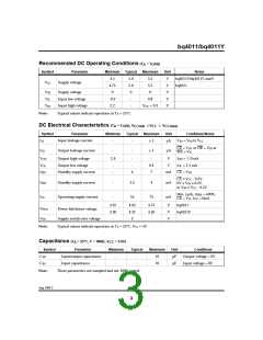
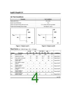
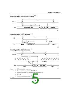
bq4011/bq4011Y
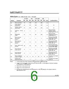
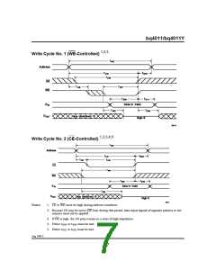
Power-Down/Power-Up Cycle (T = T
)
A
OPR
Symbol
tPF
Parameter
Minimum Typical Maximum
Unit
µs
Conditions
VCC slew, 4.75 to 4.25 V
VCC slew, 4.25 to VSO
300
10
0
-
-
-
-
-
-
tFS
µs
tPU
VCC slew, VSO to VPFD (max.)
µs
Time during which SRAM is
write-protected after VCC
passes VPFD on power-up.
tCER
Chip enable recovery time
40
80
120
ms
Data-retention time in
absence of VCC
tDR
10
-
-
years
TA = 25°C. (2)
Data-retention time in
absence of VCC
TA = 25°C (2); industrial
temperature range (-N) only.
tDR-N
6
-
-
years
Delay after VCC slews down
past VPFD before SRAM is
write-protected.
tWPT
Write-protect time
40
100
150
µs
Notes:
1. Typical values indicate operation at TA = 25°C, VCC = 5V.
2. Battery is disconnected from circuit until after VCC is applied for the first time. tDR is the
accumulated time in absence of power beginning when power is first applied to the device.
Ca u tion : Nega tive u n d er sh oots below th e a bsolu te m a xim u m r a tin g of -0.3V in ba tter y-ba ck u p m od e
m a y a ffect d a ta in tegr ity.
Power-Down/Power-Up Timing
Aug. 1993 C
8

 TI [ TEXAS INSTRUMENTS ]