bq3285ED/LD
Capacitance—bq3285ED/LD (TA = 25°C, F = 1MHz, VCC = 5.0V)
Symbol
CI/O
Parameter
Input/output capacitance
Input capacitance
Minimum
Typical
Maximum
Unit
pF
Conditions
VOUT = 0V
-
-
-
-
7
5
CIN
pF
VIN = 0V
Note:
This parameter is sampled and not 100% tested. It does not include the X1 or X2 pin.
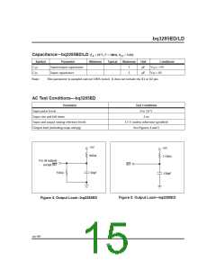
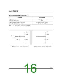
AC Test Conditions—bq3285ED
Parameter
Input pulse levels
Test Conditions
0 to 3.0 V
Input rise and fall times
5 ns
Input and output timing reference levels
Output load (including scope and jig)
1.5 V (unless otherwise specified)
See Figures 4 and 5
+5V
960
+5V
1.15k
For all outputs
except INT
INT
510
50pF
130pF
Figure 5. Output Load—bq3285ED
Figure 4. Output Load—bq3285ED
July 1997
15

 TI [ TEXAS INSTRUMENTS ]