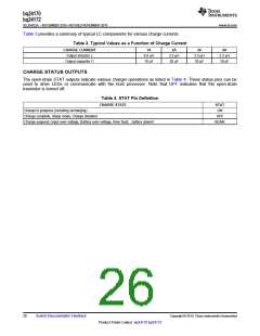
bq24170
bq24172
www.ti.com
SLUSAD2A –NOVEMBER 2010–REVISED NOVEMBER 2010
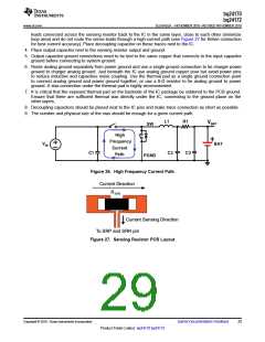
leads connected across the sensing resistor back to the IC in the same layer, close to each other (minimize
loop area) and do not route the sense leads through a high-current path (see Figure 27 for Kelvin connection
for best current accuracy). Place decoupling capacitor on these traces next to the IC.
4. Place output capacitor next to the sensing resistor output and ground.
5. Output capacitor ground connections need to be tied to the same copper that connects to the input capacitor
ground before connecting to system ground.
6. Route analog ground separately from power ground and use a single ground connection to tie charger power
ground to charger analog ground. Just beneath the IC use analog ground copper pour but avoid power pins
to reduce inductive and capacitive noise coupling. Use the thermal pad as a single ground connection point
to connect analog ground and power ground together, or use a 0-Ω resistor to tie analog ground to power
ground. A star-connection under the thermal pad is highly recommended.
7. It is critical that the exposed thermal pad on the backside of the IC package be soldered to the PCB ground.
Ensure that there are sufficient thermal vias directly under the IC, connecting to the ground plane on the
other layers.
8. Decoupling capacitors should be placed next to the IC pins and make trace connection as short as possible.
9. The number and physical size of the vias should be enough for a given current path.
L1
R1
VBAT
SW
High
Frequency
Current
Path
VIN
BAT
C1
C3
C2
PGND
Figure 26. High Frequency Current Path
Current Direction
RSNS
Current Sensing Direction
To SRP and SRN pin
Figure 27. Sensing Resistor PCB Layout
Copyright © 2010, Texas Instruments Incorporated
Submit Documentation Feedback
29
Product Folder Link(s): bq24170 bq24172

 TI [ TEXAS INSTRUMENTS ]