bq24170
bq24172
SLUSAD2A –NOVEMBER 2010–REVISED NOVEMBER 2010
www.ti.com
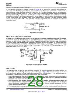
A cost effective and small size solution is shown in Figure 24. R1 and C1 are composed of a damping RC
network to damp the hot plug-in oscillation. As a result, the over-voltage spike is limited to a safe level. D1 is
used for reverse voltage protection for the AVCC pin. C2 is the AVCC pin decoupling capacitor and it should be
placed as close as possible to the AVCC pin. R2 and C2 form a damping RC network to further protect the IC
from high dv/dt and high voltage spike. The C2 value should be less than the C1 value so R1 can dominant the
equivalent ESR value to get enough damping effect for hot plug-in. R1 and R2 must be sized enough to handle
in-rush current power loss according to the resistor manufacturer’s datasheet. The filter component values
always need to be verified with a real application and minor adjustments may be needed to fit in the real
application circuit.
D1
R2(1206)
R1(2010)
2W
4.7 - 30 W
Adapter
Connector
AVCC pin
C1
2.2 mF
C2
0.1 - 1 mF
Figure 24. Input Filter
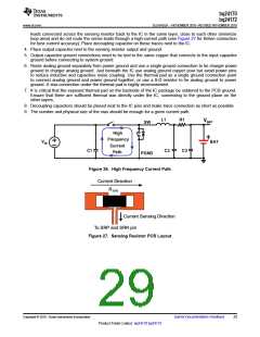
INPUT ACFET AND RBFET SELECTION
N-type MOSFETs are used as input ACFET(Q1) and RBFET(Q2) for better cost effective and small size solution,
as shown in Figure 22. Normally, there are around 50uF capacitor totally connected at PVCC node --- 10uF
capacitor for buck converter of bq24170/2 and 40uF capacitor for system side. There is a surge current during
Q1 turn-on period when a valid adapter is inserted. Decreasing the turn-on speed of Q1 can limit this surge
current in desirable range by selecting a MOSFET with relative bigger CGD and/or CGS. At the case Q1 turn on
too fast, we need add external CGD and/or CGS. For example, 4.7nF CGD and 47nF CGS are adopted on EVM
while using NexFET CSD17313 as Q1.
Q2
Q1
ADAPTER
SYS
RSNS
C4
1m
SYS
C
40
R
IN
?
2
RGS
499k
CGS
C
IN
CGD
PVCC
CMSRC
ACDRV
?
2.2
R12
4.02k
R11
4.02k
Figure 25. Input ACFET and RBFET
PCB LAYOUT
The switching node rise and fall times should be minimized for minimum switching loss. Proper layout of the
components to minimize the high frequency current path loop (see Figure 26) is important to prevent electrical
and magnetic field radiation and high frequency resonant problems. The following is a PCB layout priority list for
proper layout. Layout of the PCB according to this specific order is essential.
1. Place input capacitor as close as possible to the PVCC supply and ground connections and use the shortest
copper trace connection. These parts should be placed on the same layer of the PCB instead of on different
layers and using vias to make this connection.
2. Place the inductor input terminal as close as possible to the SW terminal. Minimize the copper area of this
trace to lower electrical and magnetic field radiation but make the trace wide enough to carry the charging
current. Do not use multiple layers in parallel for this connection. Minimize parasitic capacitance from this
area to any other trace or plane.
3. The charging current sensing resistor should be placed right next to the inductor output. Route the sense
28
Submit Documentation Feedback
Copyright © 2010, Texas Instruments Incorporated
Product Folder Link(s): bq24170 bq24172

 TI [ TEXAS INSTRUMENTS ]