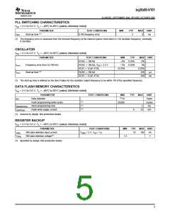
bq20z80-V101
www.ti.com
SLUS625D–SEPTEMBER 2004–REVISED OCTOBER 2005
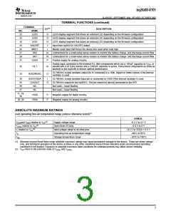
TERMINAL FUNCTIONS (continued)
TERMINAL
I/O(1)
DESCRIPTION
NO.
NAME
LED3
LED2
LED1
XALERT
MRST
SR2
22
23
24
25
26
27
28
31
O
O
O
I
LED3 display segment that drives an external LED depending on the firmware configuration
LED2 display segment that drives an external LED depending on the firmware configuration
LED1 display segment that drives an external LED depending on the firmware configuration
Input from bq29312A XALERT output.
I
Master reset input that forces the device into reset when held high
IA
IA
P
Connections for a small-value sense resistor to monitor the battery charge- and discharge-current flow
Connections for a small-value sense resistor to monitor the battery charge- and discharge-current flow
Positive supply for analog circuitry
SR1
VDDA
Analog input connected to the external PLL filter components which are a 150-pF capacitor to VSSA, in
parallel with a 61.9-kΩ resistor and a 2200-pF capacitor in series. Place these components as close as
possible to the bq20z80 to ensure optimal performance.
32
FILT
IA
32.768-kHz crystal oscillator output pin or connected to a 100k, 50ppm or better resistor if the internal
oscillator is used
33
XCK2/ROSC
O
34
35
36
37
XCK1/VSSA
CLKOUT
NC
I
O
-
32.768-kHz crystal oscillator input pin or connected to VSSA if the internal oscillator is used
32.768-kHz output for the bq29312. This pin should be directly connected to the AFE.
Not used— leave floating
NC
-
Not used— leave floating
11, 19,
38
VSSD
VSSA
P
P
Negative supply for digital circuitry
Negative supply for analog circuitry.
29, 30
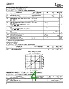
ABSOLUTE MAXIMUM RATINGS
over operating free-air temperature range (unless otherwise noted)(1)
RANGE
–0.3 V to 4.1 V
–0.3 V to 6 V
(2)
VDDAand VDDD relative to VSS
Supply voltage range
(2)
V(IOD) relative to VSS
Open-drain I/O pins
(2)
VI relative to VSS
Input voltage range to all other pins
Operating free-air temperature range
Storage temperature range
–0.3 V to VDDA + 0.3 V
–40°C to 85°C
TA
Tstg
– 65°C to 150°C
(1) Stresses beyond those listed under absolute maximum ratings may cause permanent damage to the device. These are stress ratings
only, and functional operation of the device at these or any other conditions beyond those indicated under recommended operating
conditions is not implied. Exposure to absolute-maximum-rated conditions for extended periods may affect device reliability.
(2) VSS refers to the common node of V(SSA) and V(SSD)
.
3

 TI [ TEXAS INSTRUMENTS ]