AM6548, AM6528, AM6526
ZHCSLA7B –DECEMBER 2019 –REVISED JUNE 2021
www.ti.com.cn
6.3 Signal Descriptions
Many signals are available on multiple pins, according to the software configuration of the pin multiplexing
options.
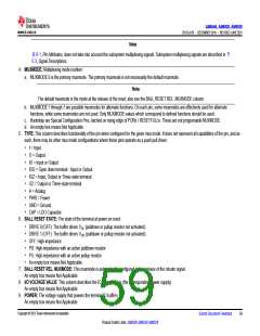
The following list describes the column headers:
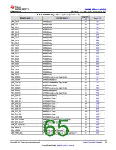
1. SIGNAL NAME: The name of the signal passing through the pin.
Note
In 表6-1 and 表6-76 are not described the subsystem multiplexing signals.
2. DESCRIPTION: Description of the signal
3. PIN TYPE: This column describes functionality of the pin when configured for the given mux mode. It does
not represent all capabilities of the pin, and as such, there may be other mux mode configurations where
these pins operate as a push-pull driver:
• I = Input
• O = Output
• IO = Input or Output
• IOD = Open drain terminal - Input or Output
• IOZ = Input, Output or Three-state terminal
• OZ = Output or Three-state terminal
• A = Analog
• PWR = Power
• GND = Ground
• CAP = LDO Capacitor
4. BALL: Associated balls bottom
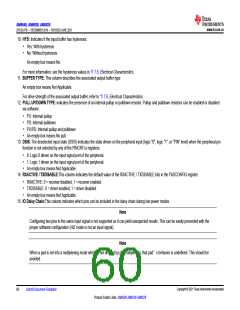
For more information on the I/O cell configurations, see the Pad Configuration Registers section in the
device TRM.
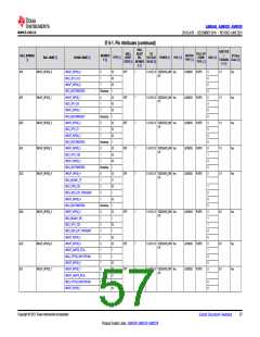
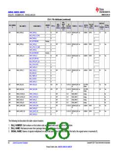
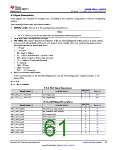
6.3.1 ADC
6.3.1.1 MCU Domain
表6-2. ADC Signal Descriptions
PIN TYPE
SIGNAL NAME [1]
DESCRIPTION [2]
BALL [4]
[3]
MCU_ADC_EXT_TRIGGER0
MCU_ADC_EXT_TRIGGER1
ADC Trigger Input
ADC Trigger Input
I
I
AC3
AD3
表6-3. ADC0 Signal Descriptions
PIN TYPE
SIGNAL NAME [1]
DESCRIPTION [2]
BALL [4]
[3]
MCU_ADC0_REFN
MCU_ADC0_REFP
MCU_ADC0_AIN0
MCU_ADC0_AIN1
MCU_ADC0_AIN2
MCU_ADC0_AIN3
MCU_ADC0_AIN4
MCU_ADC0_AIN5
MCU_ADC0_AIN6
MCU_ADC0_AIN7
ADC Reference Input (negative)
ADC Reference Input (positive)
ADC Analog Input 0
A
A
A
A
A
A
A
A
A
A
K2
K3
K5
J3
J1
J5
K4
J4
J2
J6
ADC Analog Input 1
ADC Analog Input 2
ADC Analog Input 3
ADC Analog Input 4
ADC Analog Input 5
ADC Analog Input 6
ADC Analog Input 7
Copyright © 2021 Texas Instruments Incorporated
Submit Document Feedback
61
Product Folder Links: AM6548 AM6528 AM6526

 TI [ TEXAS INSTRUMENTS ]