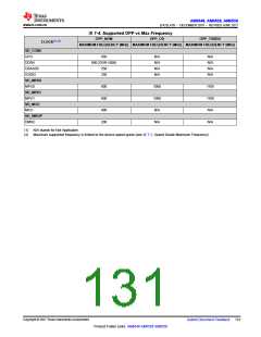
AM6548, AM6528, AM6526
ZHCSLA7B –DECEMBER 2019 –REVISED JUNE 2021
www.ti.com.cn
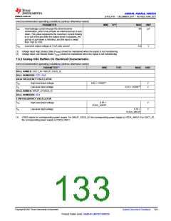
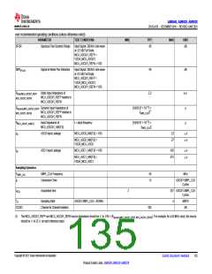
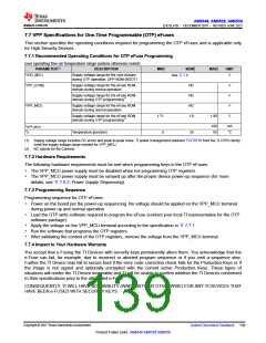
over recommended operating conditions (unless otherwise noted)
PARAMETER
TEST CONDITIONS
MIN
TYP
MAX
UNIT
SFDR
Spurious Free Dynamic Range
Input Signal: 200 kHz sine wave
at -0.5 dB Full Scale,
80
dB
MCU_ADC0/1_REFP =
VDDA_MCU_ADC0/1,
MCU_ADC0/1_REFN = VSS
SNR(PLUS)
Signal-to-Noise Plus Distortion
Input Signal: 200 kHz sine wave
at -0.5 dB Full Scale,
69
dB
MCU_ADC0/1_REFP =
VDDA_MCU_ADC0/1,
MCU_ADC0/1_REFN = VSS
Rstatic(MCU_ADC0/1_REFP,
Static Input Impedance of
MCU_ADC0/1_REFP relative to
MCU_ADC0/1_REFN
2.2
kΩ
Ω
MCU_ADC0/1_REFN)
Rdynamic(MCU_ADC0/1_REFP, Dynamic Input Impedance of
[1/((65.97 × 10-12) ×
fSMPL_CLK)](1)
MCU_ADC0/1_REFP relative to
MCU_ADC0/1_REFN)
MCU_ADC0/1_REFN
RMCU_ADC0/1_AIN[0:7]
IIN
Input Impedance of
MCU_ADC0/1_AIN[7:0]
f = input frequency
[1/((65.97 × 10-12) ×
fSMPL_CLK)]
Ω
ADC0 Input Leakage
ADC1 Input Leakage
MCU_ADC0_AIN[7:0] = VSS
-23
27
μA
μA
MCU_ADC0_AIN[7:0] =
VDDA_MCU_ADC0
IIN
MCU_ADC1_AIN[7:0] = VSS
-126
572
μA
μA
MCU_ADC1_AIN[7:0] =
VDDA_MCU_ADC1
Sampling Dynamics
FSMPL_CLK
tC
SMPL_CLK Frequency
Conversion Time
60
13
MHz
ADC0/1 SMPL_CLK
Cycles
tACQ
Acquisition time
2
257 ADC0/1 SMPL_CLK
Cycles
TR
Sampling Rate
ADC0/1 SMPL_CLK = 60 MHz
4
MSPS
dB
CCISO
Channel to Channel Isolation
100
(1) The MCU_ADC0/1_REFP and MCU_ADC0/1_REFN source impedance should be ≤to 1/10 × (Rdynamic(MCU_ADC0/1_REFP, MCU_ADC0/1_REFN)). For example, for a 60 MHz clock, this source
should be ≤to 25 Ωon each reference input.
Copyright © 2021 Texas Instruments Incorporated
Submit Document Feedback
135
Product Folder Links: AM6548 AM6528 AM6526

 TI [ TEXAS INSTRUMENTS ]