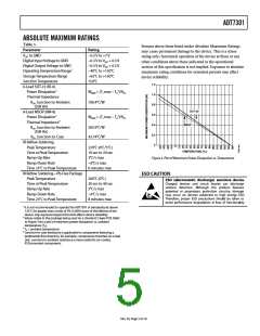
ADT7301
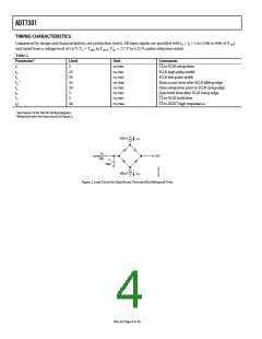
TIMING CHARACTERISTICS
Guaranteed by design and characterization, not production tested. All input signals are specified with tR = tF = 5 ns (10% to 90% of VDD
and timed from a voltage level of 1.6 V. TA = TMIN to TMAX, VDD = 2.7 V to 5.25 V, unless otherwise noted.
)
Table 2.
Parameter1
Limit
5
Unit
Comments
t1
t2
t3
ns min
ns min
ns min
ns max
ns min
ns min
ns min
ns max
CS to SCLK setup time
25
25
35
20
5
SCLK high pulse width
SCLK low pulse width
Data access time after SCLK falling edge
Data setup time prior to SCLK rising edge
Data hold time after SCLK rising edge
CS to SCLK hold time
2
t4
t5
t6
t7
5
2
t8
40
CS to DOUT high Impedance
1 See Figure 14 for the SPI timing diagram.
2 Measured with the load circuit of Figure 2.
200µA
I
OL
TO
OUTPUT
PIN
1.6V
C
L
50pF
200µA
I
OH
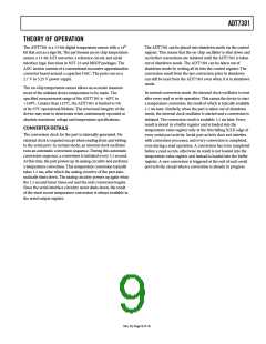
Figure 2. Load Circuit for Data Access Time and Bus Relinquish Time
Rev. B | Page 4 of 16

 TI [ TEXAS INSTRUMENTS ]