ADS7056
ZHCSG66 –MARCH 2017
www.ti.com.cn
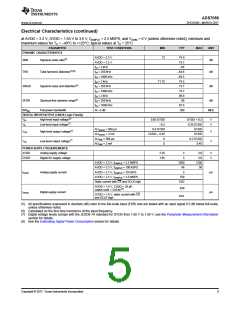
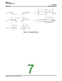
6.6 Timing Requirements
all specifications are at AVDD = 2.35 V to 3.6 V, DVDD = 1.65 V to 3.6 V, and CLOAD-SDO = 20 pF (unless otherwise noted);
minimum and maximum values for TA = –40°C to +125°C; typical values at TA = 25°C
MIN
16.66
7
TYP
MAX
UNIT
ns
tCLK
Time period of SCLK
tsu_CSCK
tht_CKCS
tph_CK
tpl_CK
Setup time: CS falling edge to SCLK falling edge
Hold time: SCLK rising edge to CS rising edge
SCLK high time
ns
8
ns
0.45
0.45
15
0.55
0.55
tSCLK
tSCLK
ns
SCLK low time
tph_CS
CS high time
6.7 Switching Characteristics
all specifications are at AVDD = 2.35 V to 3.6 V, DVDD = 1.65 V to 3.6 V, and CLOAD-SDO = 20 pF (unless otherwise noted);
minimum and maximum values for TA = –40°C to +125°C; typical values at TA = 25°C
PARAMETER
Cycle time
Conversion time
TEST CONDITIONS
MIN
TYP
MAX
UNIT
ns
(1)
tCYCLE
tCONV
400
18 × tSCLK
ns
tden_CSDO Delay time: CS falling edge to data enable
6.5
10
ns
Delay time: SCLK rising edge to (next) data
valid on SDO
td_CKDO
ns
ns
tht_CKDO
tdz_CSDO
SCLK rising edge to current data invalid
2.5
5.5
Delay time: CS rising edge to SDO going to
tri-state
(1) tCYCLE = 1 / fSAMPLE
.
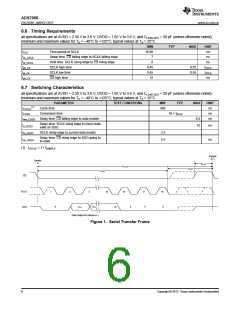
Sample
A+1
Sample
A
tph_CS
tCYCLE
tACQ
tCONV
CS
SCLK
SDO
1
2
3
15
16
17
18
0
D12
D0
0
0
0
D13
Data Output for Sample A-1
Figure 1. Serial Transfer Frame
6
Copyright © 2017, Texas Instruments Incorporated

 TI [ TEXAS INSTRUMENTS ]