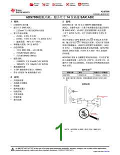
ADS7056
www.ti.com.cn
ZHCSG66 –MARCH 2017
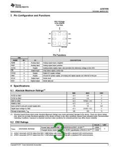
5 Pin Configuration and Functions
RUG Package
8-Pin X2QFN
Top View
CS
1
2
3
7
6
5
AINP
AVDD
GND
SDO
SCLK
Not to scale
Pin Functions
PIN
NAME
AINM
NO.
8
I/O
DESCRIPTION
Analog input
Analog input
Supply
Analog signal input, negative
Analog signal input, positive
AINP
AVDD
CS
7
6
Analog power-supply input, also provides the reference voltage to the ADC
1
Digital input
Supply
Chip-select signal, active low
DVDD
GND
SCLK
SDO
4
Digital I/O supply voltage
5
Supply
Ground for power supply, all analog and digital signals are referred to this pin
3
Digital input
Digital output
Serial clock
2
Serial data out
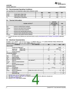
6 Specifications
6.1 Absolute Maximum Ratings(1)
MIN
–0.3
–0.3
–0.3
–0.3
–10
MAX
3.9
UNIT
V
AVDD to GND
DVDD to GND
3.9
V
AINP to GND
AVDD + 0.3
0.3
V
AINM to GND
V
Input current to any pin except supply pins
Digital input voltage to GND
Storage temperature, Tstg
10
mA
V
–0.3
–60
DVDD + 0.3
150
°C
(1) Stresses beyond those listed under Absolute Maximum Ratings may cause permanent damage to the device. These are stress ratings
only, which do not imply functional operation of the device at these or any other conditions beyond those indicated under Recommended
Operating Conditions. Exposure to absolute-maximum-rated conditions for extended periods may affect device reliability.
6.2 ESD Ratings
VALUE
±2000
±1000
UNIT
Human body model (HBM), per ANSI/ESDA/JEDEC JS-001(1)
Charged device model (CDM), per JEDEC specification JESD22-C101(2)
V(ESD)
Electrostatic discharge
V
(1) JEDEC document JEP155 states that 500-V HBM allows safe manufacturing with a standard ESD control process.
(2) JEDEC document JEP157 states that 250-V CDM allows safe manufacturing with a standard ESD control process.
Copyright © 2017, Texas Instruments Incorporated
3

 TI [ TEXAS INSTRUMENTS ]