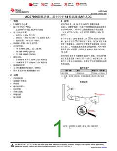
ADS7056
ZHCSG66 –MARCH 2017
www.ti.com.cn
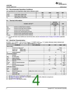
6.3 Recommended Operating Conditions
over operating free-air temperature range (unless otherwise noted)
MIN
2.35
1.65
–40
NOM
3
MAX
3.6
UNIT
V
AVDD
DVDD
TA
Analog supply voltage range
Digital supply voltage range
Operating free-air temperature
1.8
25
3.6
V
125
°C
6.4 Thermal Information
ADS7056
THERMAL METRIC(1)
RUG (X2QFN)
UNIT
8 PINS
177.5
51.5
76.7
1
RθJA
Junction-to-ambient thermal resistance
°C/W
°C/W
°C/W
°C/W
°C/W
°C/W
RθJC(top)
RθJB
Junction-to-case (top) thermal resistance
Junction-to-board thermal resistance
ψJT
Junction-to-top characterization parameter
Junction-to-board characterization parameter
Junction-to-case (bottom) thermal resistance
ψJB
76.7
N/A
RθJC(bot)
(1) For more information about traditional and new thermal metrics, see the Semiconductor and IC Package Thermal Metrics application
report.
6.5 Electrical Characteristics
at AVDD = 3.3 V, DVDD = 1.65 V to 3.6 V, fSAMPLE = 2.5 MSPS, and VAINM = 0 V (unless otherwise noted); minimum and
maximum values for TA = –40°C to +125°C; typical values at TA = 25°C
PARAMETER
TEST CONDITIONS
MIN
TYP
MAX
UNIT
ANALOG INPUT
Full-scale input voltage span(1)
0
–0.1
–0.1
AVDD
AVDD + 0.1
0.1
V
V
AINP to GND
AINM to GND
Absolute input
voltage range
CS
Sampling capacitance
16
14
pF
SYSTEM PERFORMANCE
Resolution
Bits
Bits
LSB(3)
NMC
INL(2)
DNL
No missing codes
14
–3
Integral nonlinearity
Differential nonlinearity
Offset error
±2
±0.5
±2.5
1.75
±0.01
0.5
3
1
6
–0.99
–6
LSB
(2)
EO
After calibration(4)
LSB
dVOS/dT
Offset error drift with temperature
Gain error
ppm/°C
%FS
(2)
EG
–0.1
95
0.1
Gain error drift with temperature
ppm/°C
SAMPLING DYNAMICS
tCONV Conversion time
tACQ
18 × tSCLK
ns
ns
Acquisition time
fSAMPLE
Maximum throughput rate
Aperture delay
60-MHz SCLK, AVDD = 2.35 V to 3.6 V
2.5
MHz
ns
3
Aperture jitter, RMS
12
ps
(1) Ideal input span; does not include gain or offset error.
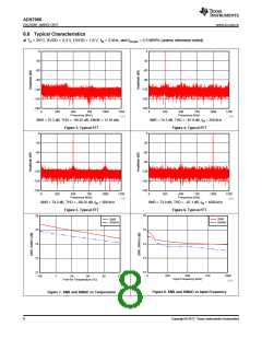
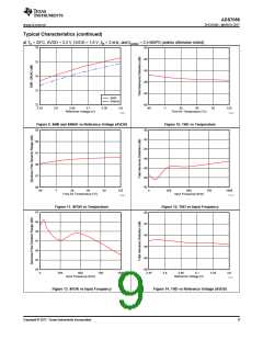
(2) See Figure 32, Figure 33, and Figure 34 for statistical distribution data for INL, offset error, and gain error.
(3) LSB means least significant bit.
(4) See the OFFCAL State section for details.
4
Copyright © 2017, Texas Instruments Incorporated

 TI [ TEXAS INSTRUMENTS ]