ADS131M04-Q1
ZHCSOL7A –MARCH 2022 –REVISED AUGUST 2022
www.ti.com.cn
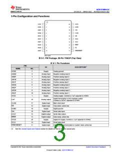
5 Pin Configuration and Functions
AVDD
AGND
AIN0P
AIN0N
AIN1N
AIN1P
AIN2P
AIN2N
AIN3N
AIN3P
1
2
3
4
5
6
7
8
9
10
20
19
18
17
16
15
14
13
12
11
DVDD
DGND
CAP
CLKIN
DIN
DOUT
SCLK
DRDY
CS
SYNC/RESET
Not to scale
图5-1. PW Package, 20-Pin TSSOP (Top View)
表5-1. Pin Functions
PIN
I/O
DESCRIPTION(1)
NAME
AGND
NO.
2
Supply
Analog ground
AIN0N
AIN0P
AIN1N
AIN1P
AIN2N
AIN2P
AIN3N
AIN3P
AVDD
4
Analog input
Analog input
Analog input
Analog input
Analog input
Analog input
Analog input
Analog input
Supply
Negative analog input 0
Positive analog input 0
3
5
Negative analog input 1
Positive analog input 1
6
8
Negative analog input 2
Positive analog input 2
7
9
Negative analog input 3
Positive analog input 3
10
1
Analog supply. Connect a 1-µF capacitor to AGND.
Digital low-dropout (LDO) regulator output.
Connect a 220-nF capacitor to DGND.
CAP
18
Analog output
CLKIN
CS
17
12
19
16
15
13
20
14
11
Digital input
Digital input
Supply
Main clock input
Chip select; active low
DGND
DIN
Digital ground
Digital input
Digital output
Digital output
Supply
Serial data input
DOUT
DRDY
DVDD
SCLK
Serial data output
Data ready; active low
Digital I/O supply. Connect a 1-µF capacitor to DGND.
Serial data clock
Digital input
Digital input
SYNC/RESET
Conversion synchronization or system reset; active low
(1) See the Unused Inputs and Outputs section for details on how to connect unused pins.
Copyright © 2022 Texas Instruments Incorporated
Submit Document Feedback
3
Product Folder Links: ADS131M04-Q1

 TI [ TEXAS INSTRUMENTS ]