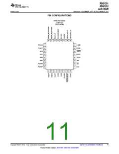
ADS1291
ADS1292
ADS1292R
SBAS502A –DECEMBER 2011–REVISED MARCH 2012
www.ti.com
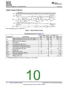
TIMING CHARACTERISTICS
tCLK
CLK
tCSSC
tCSH
tSDECODE
tSPWL
CS
tSCCS
tSCLK
tSPWH
SCLK
1
2
3
8
1
2
3
8
tDIHD
tDIST
tDOPD
DIN
tCSDOZ
Hi-Z
tCSDOD
Hi-Z
DOUT
NOTE: SPI settings are CPOL = 0 and CPHA = 1.
Figure 1. Serial Interface Timing
Timing Requirements For Figure 1(1)
2.7 V ≤ DVDD ≤ 3.6 V
1.7 V ≤ DVDD ≤ 2 V
PARAMETER
DESCRIPTION
Master clock period (CLK_DIV bit of LOFF_STAT register = 0)
Master clock period (CLK_DIV bit of LOFF_STAT register = 1)
CS low to first SCLK, setup time
SCLK period
MIN
1775
444
6
TYP
MAX
2170
542
MIN
1775
444
17
TYP
MAX UNIT
2170
542
ns
ns
tCLK
tCSSC
ns
tSCLK
50
66.6
25
ns
tSPWH, L
tDIST
SCLK pulse width, high and low
DIN valid to SCLK falling edge: setup time
Valid DIN after SCLK falling edge: hold time
SCLK rising edge to DOUT valid
CS high pulse
15
ns
10
10
ns
tDIHD
10
11
ns
tDOPD
tCSH
tCSDOD
tSCCS
tSDECODE
tCSDOZ
12
10
22
20
ns
2
10
3
2
20
3
tCLKs
ns
CS low to DOUT driven
Eighth SCLK falling edge to CS high
Command decode time
tCLKs
tCLKs
ns
4
4
CS high to DOUT Hi-Z
(1) Specifications apply from –40°C to +85°C. Load on DOUT = 20 pF || 100 kΩ.
10
Submit Documentation Feedback
Copyright © 2011–2012, Texas Instruments Incorporated
Product Folder Link(s): ADS1291 ADS1292 ADS1292R

 TI [ TEXAS INSTRUMENTS ]