ADC0801, ADC0802
ADC0803, ADC0804, ADC0805
www.ti.com
SNOSBI1B –NOVEMBER 2009–REVISED FEBRUARY 2013
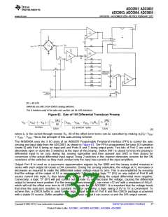
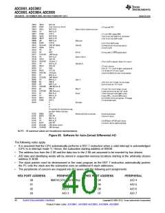
R2 = 49.5 R1
Switches are LMC13334 CMOS analog switches.
The 9 resistors used in the auto-zero section can be ±5% tolerance.
Figure 62. Gain of 100 Differential Transducer Preamp
(5)
where IX is the current through resistor RX. All of the offset error terms can be cancelled by making ±IXRX= VOS1
+ VOS3 − VOS2. This is the principle of this auto-zeroing scheme.
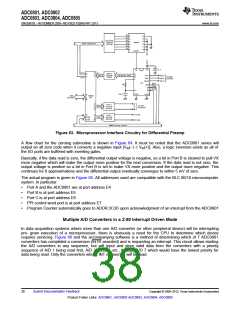
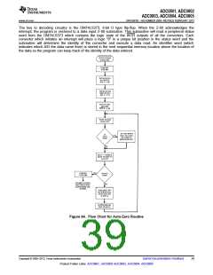
The INS8080A uses the 3 I/O ports of an INS8255 Programable Peripheral Interface (PPI) to control the auto
zeroing and input data from the ADC0801 as shown in Figure 63. The PPI is programmed for basic I/O operation
(mode 0) with Port A being an input port and Ports B and C being output ports. Two bits of Port C are used to
alternately open or close the 2 switches at the input of the preamp. Switch SW1 is closed to force the preamp’s
differential input to be zero during the zeroing subroutine and then opened and SW2 is then closed for
conversion of the actual differential input signal. Using 2 switches in this manner eliminates concern for the ON
resistance of the switches as they must conduct only the input bias current of the input amplifiers.
Output Port B is used as a successive approximation register by the 8080 and the binary scaled resistors in
series with each output bit create a D/A converter. During the zeroing subroutine, the voltage at Vx increases or
decreases as required to make the differential output voltage equal to zero. This is accomplished by ensuring
that the voltage at the output of A1 is approximately 2.5V so that a logic "1" (5V) on any output of Port B will
source current into node VX thus raising the voltage at VX and making the output differential more negative.
Conversely, a logic "0" (0V) will pull current out of node VX and decrease the voltage, causing the differential
output to become more positive. For the resistor values shown, VX can move ±12 mV with a resolution of 50 µV,
which will null the offset error term to /⁄4 LSB of full-scale for the ADC0801. It is important that the voltage levels
that drive the auto-zero resistors be constant. Also, for symmetry, a logic swing of 0V to 5V is convenient. To
achieve this, a CMOS buffer is used for the logic output signals of Port B and this CMOS package is powered
with a stable 5V source. Buffer amplifier A1 is necessary so that it can source or sink the D/A output current.
Copyright © 2009–2013, Texas Instruments Incorporated
Submit Documentation Feedback
37
Product Folder Links: ADC0801, ADC0802 ADC0803, ADC0804, ADC0805

 TI [ TEXAS INSTRUMENTS ]