SN54173, SN54LS173A, SN74173, SN74LS173A
4-BIT D-TYPE REGISTERS
WITH 3-STATE OUTPUTS
SDLS067A – OCTOBER 1976 – REVISED JUNE 1999
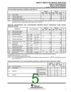
recommended operating conditions (see Note 3)
SN54173
SN74173
UNIT
MIN NOM
MAX
5.5
–2
MIN NOM
MAX
5.25
–5.2
16
V
Supply voltage
4.5
5
4.75
5
V
CC
OH
OL
I
I
High-level output current
Low-level output current
Operating free-air temperature
mA
mA
°C
16
T
A
–55
125
0
70
NOTE 3: All unused inputs of the device must be held at V
or GND to ensure proper device operation. Refer to the TI application report,
CC
Implications of Slow or Floating CMOS Inputs, literature number SCBA004.
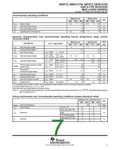
electrical characteristics over recommended operating free-air temperature range (unless
otherwise noted)
SN54173
SN74173
†
PARAMETER
UNIT
TEST CONDITIONS
‡
‡
MIN TYP
MAX
MIN TYP
MAX
V
V
V
High-level input voltage
Low-level input voltage
Input clamp voltage
2
2
V
V
V
IH
0.8
0.8
IL
V
= MIN,
= MIN,
I = –12 mA
–1.5
–1.5
IK
CC
I
V
V
V
= 2 V,
= MAX
CC
IL
IH
V
High-level output voltage
Low-level output voltage
2.4
2.4
V
V
OH
OL
= 0.8 V,
I
OH
V
V
= MIN,
= 0.8 V,
V
= 2 V,
= 16 mA
CC
IL
IH
V
0.4
0.4
I
OL
V
= 2.4 V
= 0.4 V
150
40
Off-state (high-impedance state)
output current
V
V
= MAX,
= 2 V
O
O
CC
IH
I
I
µA
O(off)
I
V
–150
–40
Input current
at maximum input voltage
V
CC
= MAX,
V = 5.5 V
I
1
1
mA
I
I
I
I
High-level input current
Low-level input current
V
CC
V
CC
V
CC
V
CC
= MAX,
= MAX,
= MAX
= MAX,
V = 2.4 V
40
–1.6
–70
72
40
–1.6
–70
72
µA
mA
mA
mA
IH
I
V = 0.4 V
I
IL
§
Short-circuit output current
Supply current
–30
–30
OS
CC
See Note 4
50
50
†
‡
§
For conditions shown as MIN or MAX, use the appropriate value specified under recommended operating conditions.
All typical values are at V = 5 V, T = 25°C.
Not more than one output should be shorted at a time.
CC
A
NOTE 4:
I
ismeasuredwithalloutputsopen;CLRgrounded,followingmomentaryconnectionto4.5V, N, G1, G2,andalldatainputsgrounded;
CC
and CLK and M at 4.5 V.
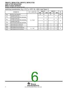
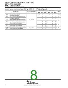
timing requirements over recommended operating conditions (unless otherwise noted)
SN54173
SN74173
UNIT
MIN
MAX
25
MIN
MAX
25
f
t
Input clock frequency
Pulse duration
MHz
ns
clock
CLK or CLR
20
17
10
10
2
20
17
10
10
2
w
Data enable (G1, G2)
Data
t
Setup time
Hold time
ns
ns
su
h
CLR (inactive state)
Data enable (G1, G2)
Data
t
10
10
5
POST OFFICE BOX 655303 • DALLAS, TEXAS 75265

 TI [ TEXAS INSTRUMENTS ]