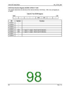
73S1215F Data Sheet
DS_1215F_003
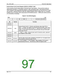
Smart Card Control Register (SCCtl): 0xFE0A Å 0x21
This register is used to monitor reception of data from the smart card.
Table 90: The SCCtl Register
MSB
LSB
CLKLVL CLKOFF
RSTCRD
–
IO
IOD
C8
C4
Bit
Symbol
Function
1 = Asserts the RST (set RST = 0) to the smart card interface, 0 = De-
assert the RST (set RST = 1) to the smart card interface. Can be used to
extend RST to the smart card. Refer to the RLength register description.
This bit is operational in all modes and can be used to extend RST during
activation or perform a “Warm Reset” as required. In auto-sequence
mode, this bit should be set = 0 to allow the sequencer to de-assert RST
per the RLength parameters.
SCCtl.7
RSTCRD
In sync mode (see the SPrtcol register) the sense of this bit is non-
inverted, if set =1 , RST = 1, if set = 0, RST = 0. Rlen has no effect on
Reset in sync mode.
SCCtl.6
SCCtl.5
–
Smart Card I/O. Read is state of I/O signal (Caution, this signal is not
synchronized to the MPU clock). In Bypass mode, write value is state of
signal on I/O. In sync mode, this bit will contain the value of I/O pin on
the latest rising edge of CLK.
IO
Smart Card I/O Direction control Bypass mode or sync mode. 1 = input
(default), 0 = output.
SCCtl.4
SCCtl.3
IOD
C8
Smart Card C8. When C8 is an output, the value written to this bit will
appear on the C8 line. The value read when C8 is an output is the value
stored in the register. When C8 is an input, the value read is the value
on the C8 pin (Caution, this signal is not synchronized to the MPU clock).
When C8 is an input, the value written will be stored in the register but
not presented to the C8 pin.
Smart Card C4. When C4 is an output, the value written to this bit will
appear on the C4 line. The value read when C4 is an output is the value
stored in the register. When C4 is an input, the value read is the value
on the C4 pin (Caution, this signal is not synchronized to the MPU clock).
When C4 is an input, the value written will be stored in the register but
not presented to the C4 pin.
SCCtl.2
C4
1 = High, 0 = Low. If CLKOFF is set = 1, the CLK to smart card will be at
the logic level indicated by this bit. If in bypass mode, this bit directly
controls the state of CLK.
SCCtl.1
SCCtl.0
CLKLVL
CLKOFF
0 = CLK is enabled. 1 = CLK is not enabled. When asserted, the CLK
will stop at the level selected by CLKLVL. This bit has no effect if in
bypass mode.
96
Rev. 1.4

 TERIDIAN [ TERIDIAN SEMICONDUCTOR CORPORATION ]