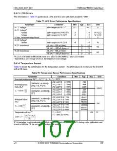
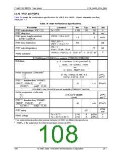
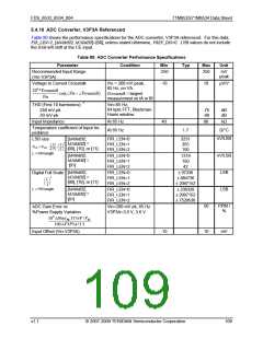
71M6533/71M6534 Data Sheet
FDS_6533_6534_004
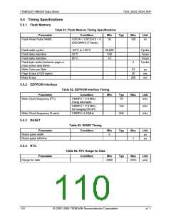
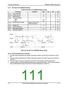
5.5 Timing Specifications
5.5.1 Flash Memory
Table 81: Flash Memory Timing Specifications
Parameter
Condition
Min
Typ
Max
Unit
Flash Read Pulse Width
V3P3A = V3P3SYS = 0
(BROWNOUT Mode)
30
100
ns
Flash write cycles
Flash data retention
Flash data retention
-40°C to +85°C
25°C
20,000
100
Cycles
Years
Years
Cycles
85°C
10
Flash byte writes between page or
mass erase operations
2
Write Time per Byte
Page Erase (1024 bytes)
Mass Erase
42
20
µs
ms
ms
200
5.5.2 EEPROM Interface
Table 82: EEPROM Interface Timing
Parameter
Write Clock frequency (I2C)
Condition
Min
Typ
Max
Unit
CKMPU = 4.9 MHz,
Using interrupts
78
kHz
CKMPU = 4.9 MHz,
bit-banging DIO4/5
150
500
kHz
kHz
Write Clock frequency (3-wire)
CKMPU=4.9 MHz
5.5.3 RESET
Table 83: RESET Timing
Condition
Parameter
Reset pulse width
Min
Typ
Max
Unit
µs
5
Reset pulse fall time
1
µs
5.5.4 RTC
Table 84: RTC Range for Date
Condition
Parameter
Min
Typ
Max
Unit
Range for date
2000
-
2255
year
110
© 2007-2009 TERIDIAN Semiconductor Corporation
v1.1

 TERIDIAN [ TERIDIAN SEMICONDUCTOR CORPORATION ]