FDS_6533_6534_004
71M6533/71M6534 Data Sheet
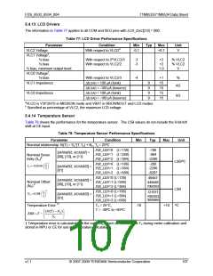
5.4.13 LCD Drivers
The information in Table 77 applies to all COM and SEG pins with LCD_DAC[2:0] = 000.
Table 77: LCD Driver Performance Specifications
Parameter
Condition
Min
Typ
Max
Unit
VLC2 Voltage
With respect to VLCDa
-0.1
+0.1
V
VLC1 Voltage†,
⅓ bias
With respect to 2*VLC2/3
With respect to VLC2/2
-3
-3
+2
+2
1.0
% VLC2
% VLC2
V
½ bias
½ bias, minimum output level
VLC0 Voltage†,
⅓ bias
With respect to VLC2/3
∆ILOAD = 100 µA (Isink)
∆ILOAD = -100 µA (Isource)
∆ILOAD = 100 µA (Isink)
∆ILOAD = -100 µA (Isource)
-4
+1
15
15
15
15
%
VLC1 Impedance
VLC0 Impedance
9
9
9
9
kΩ
kΩ
aVLCD is V3P3SYS in MISSION mode and VBAT in BROWNOUT and LCD modes.
† Specified as percentage of VLC2, the maximum LCD voltage.
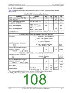
5.4.14 Temperature Sensor
Table 78 shows the performance for the temperature sensor. The LSB values do not include the 8-bit left
shift at CE input.
Table 78: Temperature Sensor Performance Specifications
Parameter
Condition
Min
Typ
Max
Unit
Nominal relationship: N(T) = Sn*(T-Tn) + Nn, Tn = 25ºC
FIR_LEN=0 (L=138)
FIR_LEN=1 (L=288)
FIR_LEN=2 (L=384)
-106
-964
-2286
[M40MHZ, M26MH] =
[00], [10], or [11]
Nominal Sensi-
tivity (Sn)4
LSB/ºC
3
FIR_LEN=0 (L=186)
FIR_LEN=1 (L=384)
FIR_LEN=2 (L=588)
-260
-2286
-8207
L
S = −0.00109⋅
n
[M40MHZ, M26MHZ] =
[01]
3
FIR_LEN=0 (L=138)
FIR_LEN=1 (L=288)
FIR_LEN=2 (L=384)
49447
449446
1065353
[M40MHZ, M26MHZ] =
[00], [10], or [11]
Nominal Offset
(Nn) 4
LSB
ºC
3
L
FIR_LEN=0 (L=186)
FIR_LEN=1 (L=384)
FIR_LEN=2 (L=588)
121071
1065353
3825004
Nn = 0.508⋅
[M40MHZ, M26MHZ] =
[01]
3
Temperature Error 1†
Tn = 25°C,
-10
+10
T = -40ºC to +85ºC
(N(T) − Nn )
ERR = T −
Sn
† Temperature error is calculated with the value Nn, which is measured at Tn during meter calibration and
stored in MPU or CE for use in temperature calculations.
v1.1
© 2007-2009 TERIDIAN Semiconductor Corporation
107

 TERIDIAN [ TERIDIAN SEMICONDUCTOR CORPORATION ]