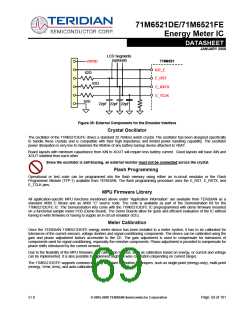
71M6521DE/71M6521FE
Energy Meter IC
DATASHEET
JANUARY 2008
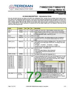
DIO_DIR1[7:6,
3:0]
SFR91
[7:6,3:0]
0
0
0
0
R/W Programs the direction of pins DIO15-DIO14, DIO11-DIO8. 1 indi-
cates output. Ignored if the pin is not configured as I/O.
DIO_DIR2
[5:3,2:1]
SFRA1
[5:3,2:1]
Programs the direction of pins DIO17-DIO16 (and DIO19-DIO21 for
R/W
the QFN package). 1 indicates output. Ignored if the pin is not con-
figured as I/O.
DIO_0[7:4,2:0]
DIO_1[7:6,3:0]
DIO_2[5:3,1:0]
DIO_EEX[1:0]
SFR80
[7:4,2:0]
0
0
0
0
0
0
The value on the pins DIO7-DIO4 and DIO2-DIO1. Pins configured
R/W
as LCD will read zero. When written, changes data on pins confi-
gured as outputs. Pins configured as LCD or input will ignore write
operations. The pushbutton input PB is read on DIO_0[0].
SFR90
[7:6,3:0]
The value on the pins DIO15-DIO14 and DIO11-DIO8. Pins con-
R/W
figured as LCD will read zero. When written, changes data on pins
configured as outputs. Pins configured as LCD or input will ignore
write operations.
SFRA0
[5:3,1:0]
The value on the pins DIO17-DIO16 (and DIO19-DIO21 for the QFN
R/W
package). Pins configured as LCD will read zero. When written,
changes data on pins configured as outputs. Pins configured as
LCD or input will ignore write operations.
When set, converts DIO4 and DIO5 to interface with external
EEPROM. DIO4 becomes SDCK and DIO5 becomes bi-directional
2008[7:6]
0
0
R/W
SDATA. LCD_NUM must be less than or equal to 18.
DIO_EEX[1:0]
Function
00
01
10
11
Disable EEPROM interface
2-Wire EEPROM interface
3-Wire EEPROM interface
--not used--
DIO_PV
DIO_PW
2008[2]
2008[3]
0
0
0
0
R/W Causes VARPULSE to be output on DIO7, if DIO7 is configured as
output. LCD_NUM must be less than 15.
R/W Causes WPULSE to be output on DIO6, if DIO6 is configured as
output. LCD_NUM must be less than 16.
EEDATA[7:0]
EECTRL[7:0]
ECK_DIS
SFR9E
SFR9F
2005[5]
0
0
0
0
0
0
R/W Serial EEPROM interface data
R/W Serial EEPROM interface control
R/W Emulator clock disable. When one, the emulator clock is disabled.
This bit is to be used with caution! Inadvertently
setting this bit will inhibit access to the part with the
ICE interface and thus preclude flash erase and pro-
gramming operations. If ECK_ENA is set, it should be done at
least 1000ms after power-up to give emulators and programming
devices enough time to complete an erase operation.
R/W Specifies the power equation to be used by the CE.
R/W Interrupt enable bits. These bits enable the XFER_BUSY, the
RTC_1SEC, the FirmWareCollision, and PLL interrupts. Note that if
one of these interrupts is to be enabled, its corresponding EX enable
bit must also be set. See the Interrupts section for details.
EQU[2:0]
EX_XFR
EX_RTC
EX_FWCOL
EX_PLL
2000[7:5]
2002[0]
2002[1]
2007[4]
2007[5]
0
0
0
0
0
0
0
0
0
0
FIR_LEN
2005[4]
0
0
R/W The length of the ADC decimation FIR filter.
1-384 cycles, 0-288 cycles
When FIR_LEN=1, the ADC has 2.370370x higher gain.
v1.0
© 2005-2008 TERIDIAN Semiconductor Corporation
Page: 73 of 101

 TERIDIAN [ TERIDIAN SEMICONDUCTOR CORPORATION ]