71M6521DE/71M6521FE
Energy Meter IC
DATASHEET
JANUARY 2008
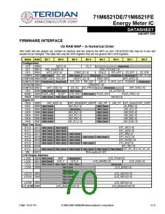
I/O RAM DESCRIPTION – Alphabetical Order
Bits with a W (write) direction are written by the MPU into configuration RAM. Typically, they are initially stored in flash memory
and copied to the configuration RAM by the MPU. Some of the more frequently programmed bits are mapped to the MPU SFR
memory space. The remaining bits are mapped to the address range 0x2xxx. Bits with R (read) direction can be read by the
MPU. Columns labeled “Rst” and “Wk” describe the bit values upon reset and wake, respectively. No entry in one of these
columns means the bit is either read-only or is powered by the non-volatile supply and is not initialized. Write-only bits will
return zero when they are read.
Name
Location
Rst Wk
Dir
Description
ADC_E
BME
2005[3]
2020[6]
0
0
0
-
R/W Enables ADC and VREF. When disabled, removes bias current
R/W Battery Measure Enable. When set, a load current is immediately
applied to the battery and it is connected to the ADC to be measured
on Alternative Mux Cycles. See MUX_ALT bit.
CE_E
2000[4]
0
0
R/W CE enable.
CE_LCTN[4:0]
20A8[4:0]
31
31
CE program location. The starting address for the CE program is
R/W
1024*CE_LCTN. CE_LCTN must be defined before the CE is en-
abled.
Chop enable for the reference bandgap circuit. The value of CHOP
CHOP_E[1:0]
2002[5:4]
0
0
R/W
will change on the rising edge of MUXSYNC according to the value
in CHOP_E:
00-toggle1 01-positive 10-reversed 11-toggle
1except at the mux sync edge at the end of SUMCYCLE.
CKOUT_E[1:0]
COMP_STAT[0]
2004[5,4]
2003[0]
CKTEST Enable. The default is 00
R/W
00
--
00
--
00-SEG19,
01-CK_FIR (5MHz Mission, 32kHz Brownout)
10-Not allowed (reserved for production test)
11-Same as 10.
R
The status of the power fail comparator for V1.
DI_RPB[2:0]
DIO_R1[2:0]
DIO_R2[2:0]
DIO_R4[2:0]
DIO_R5[2:0]
DIO_R6[2:0]
DIO_R7[2:0]
DIO_R8[2:0]
DIO_R9[2:0]
DIO_R10[2:0]
DIO_R11[2:0]
2009[2:0]
2009[6:4]
200A[2:0]
200B[2:0]
200B[6:4]
200C[2:0]
200C[6:4]
200D[2:0]
200D[6:4]
200E[2:0]
200E[6:4]
0
0
0
0
0
0
0
0
0
0
0
0
0
0
0
0
0
0
0
0
0
0
R/W
Connects dedicated I/O pins DIO2 and DIO4 through DIO11 as well
as input pins PB and DIO1 to internal resources. If more than one
input is connected to the same resource, the ‘MULTIPLE’ column
below specifies how they are combined.
DIO_Rx
000
Resource
NONE
MULTIPLE
--
001
Reserved
OR
010
011
100
101
110
111
T0 (Timer0 clock or gate)
T1 (Timer1 clock or gate)
High priority IO interrupt (int0 rising)
Low priority IO interrupt (int1 rising)
High priority IO interrupt (int0 falling)
Low priority IO interrupt (int1 falling)
OR
OR
OR
OR
OR
OR
DIO_DIR0[7:4,2:1] SFRA2
0
0
R/W Programs the direction of pins DIO7-DIO4 and DIO2-DIO1. 1 indi-
cates output. Ignored if the pin is not configured as I/O. See
DIO_PV and DIO_PW for special option for DIO6 and DIO7 outputs.
See DIO_EEX for special option for DIO4 and DIO5.
[7:4,2:0]
Page: 72 of 101
© 2005-2008 TERIDIAN Semiconductor Corporation
v1.0

 TERIDIAN [ TERIDIAN SEMICONDUCTOR CORPORATION ]