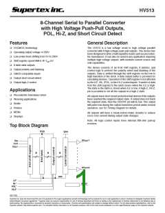
HV513
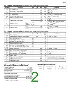
DC Electrical Characteristics (Over operating supply voltages unless otherwise noted)
Symbol
Parameter
Min
Typ
Max
Units
Conditions
IDD
VDD supply current
4
mA
fCLK=8MHz, LE*=LOW
0.1
2.0
100
100
10
All VIN=VDD
IDDQ
Quiescent VDD supply current
mA
All VIN=0V
IPP
IPPQ
IIH
VPP supply current
Quiescent VPP supply current
High-level logic input current
µA
µA
µA
VPP=250V, fOUT=300Hz, no load
VPP=240V, outputs static
VIH=VDD
-10
-350
VIL=0V
IIL
Low-level logic input current
High-level output
µA
V
VIL=0V, for inputs w/pull-up resistors
VPP =200V, IHVOUT=-20mA
IDOUT=-0.1mA
VDD =4.5V, IHVOUT=20mA
IDOUT=0.1mA
HVOUT
Data out
HVOUT
140
VDD-1V
VOH
VOL
60
1.0
Low-level output
V
Data out
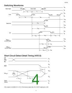
DC Electrical Characteristics (Over operating supply voltages unless otherwise noted)
Symbol
fCLK
fOUT
tW
Parameter
Min
Typ
Max
Units
MHz
Hz
ns
Conditions
Clock frequency
Output switching frequency (SOA limited)
Clock width high and low
0
8
300
CL=50nF, VPP=200V
62
15
30
80
35
40
tSU
tH
Data setup time before clock rises
Data hold time after clock rises
ns
ns
tWLE
tDLE
tSLE
Width of latch enable pulse
/LE delay time after rising edge of clock
/LE setup time before rising edge of clock
ns
ns
ns
tOR, tOF Rise/fall time of HVOUT
td ON/OFF Delay time for output to start rise/fall
1000
500
110
110
5
500
1000
500
µs
ns
ns
ns
ns
ns
ns
ns
CL=100nF, VPP=200V
tDHL
tDLH
tR, tF
tSD
tSC
tHI-Z
Delay time clock to DOUT high to low
Delay time clock to DOUT low to high
All logic inputs
Output short circuit detection
Output short circuit clear
Output high-Z state
CL=15pF
CL=15pF
Short to output fall of /SHORT, CL=15pF
Short clear to output rise of /SHORT
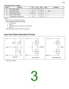
Ordering Information
Absolute Maximum Ratings*
Device
Part Number
Package
Supply Voltage, VDD
-0.5V to 6V
VDD to 275V
Supply Voltage, VPP
HV513
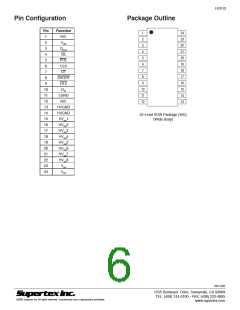
HV513WG
24 Lead SOW
Logic input levels
Ground current
-0.5V to VDD+0.5V
0.3A
High voltage supply current
Continuous total power dissipation
Operating temperature range
Storage temperature range
* All voltages are referenced to device ground.
0.25A
750mW
-40°C to +85°C
-65°C +150°C
2

 SUPERTEX [ Supertex, Inc ]