HV300
___________________________________________________________________________________________________
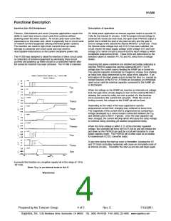
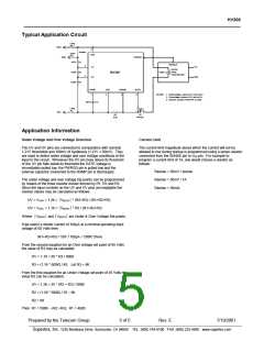
Functional Description
Insertion into Hot Backplanes
Description of operation
Telecom, Data Network and some Computer applications require the
ability to insert and remove circuit cards from systems without
powering down the entire system. All circuit cards have some filter
capacitance on the power rails, which is especially true in circuit cards
or network terminal equipment utilizing distributed power systems.
The insertion can result in high inrush currents that can cause
damage to connector and circuit cards and may result in
On initial power application an internal regulator seeks to provide 10
Volts for the internal IC circuitry. Until the proper internal voltage is
achieved all circuits are held reset, the open drain PWRGD output is
pulled low to inhibit the start of any load circuitry and the gate to
source voltage of the external N-channel MOSFET is held low. Once
the internal under voltage lock out (UVLO) has been satisfied, the
circuit checks the input supply voltage under voltage (UV) and over
voltage (OV) sense circuits to ensure that the input voltage is within
acceptable programmed limits. These limits are determined by the
selected values of resistors R1, R2 and R3, which form a voltage
divider.
unacceptable disturbances on the system backplane power rails.
The HV300 was designed to allow the insertion of these circuit cards
or connection of terminal equipment by eliminating these inrush
currents and powering up these circuits in a controlled manner after
full connector insertion has been achieved. The HV300 is intended
Assuming the above conditions are satisfied and while continuing to
hold the PWRGD output low and the external MOSFET GATE
voltage low, the current source feeding the RAMP pin is turned on.
The external capacitor connected to it begins to charge, thus starting
an initial time delay determined by the value of the capacitor. If an
interruption of the input power occurs during this time (i.e. caused by
contact bounce) or the OV or UV limits are exceeded, an immediate
reset occurs and the external capacitor connected to the RAMP pin
is discharged.
VDD
UV
When the voltage on the RAMP pin reaches an internally set voltage
limit, the gate drive circuitry begins to turn on the external MOSFET;
allowing the current to softly rise over a period of a few hundred
micro-seconds to the current limit set point. While the circuit is
limiting current, the voltage on the RAMP pin will be fixed.
VSENSE
Depending on the value of the load capacitance and the
programmed current limit, charging may continue for some time.
The magnitude of the current limit is programmed by comparing a
voltage developed by a sense resistor connected between the VEE
and SENSE pins to 50mV (Typical). Once the load capacitor has
been charged, the current will drop which will cause the ramp voltage
to continue rising; providing yet another programmed delay.
VRAMP
VGATE
VPWRGD
When the ramp voltage is within 1.2V of the internally regulated
voltage, the controller will force the GATE full on and will release the
pull down on the PWRGD pin and the circuit will transition to a low
power standby mode. The PWRGD pin is often used as an enable
for downstream DC/DC converter loads.
VDD1
At any time during the start up cycle or thereafter, crossing the UV
and OV limits (including hysteresis) will cause an immediate reset of
all internal circuitry. Thereafter the start up process will begin again.
VDRAIN
ILIMIT
to provide this function on a negative supply rail in the range of -10 to
-90 Volts.
Note: VDD1 is an internal node in the IC
Waveforms
Prepared by the Telecom Group
4 of 5
Rev. E
7/19/2001
_________________________________________________________________ ______________________________________________
Supertex, Inc. 1235 Bordeaux Drive, Sunnyvale, CA 94089 TEL: (408) 744-0100 FAX: (408) 222-4895 www.supertex.com

 SUPERTEX [ Supertex, Inc ]