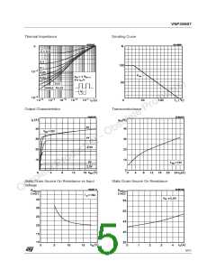
VNP35N07
ELECTRICAL CHARACTERISTICS (continued)
SWITCHING ( )
Symbol
Parameter
Test Conditions
Min.
Typ.
Max.
Unit
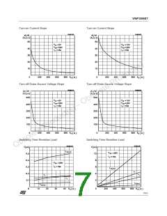
td(on)
tr
td(off)
tf
Turn-on Delay Time
Rise Time
Turn-off Delay Time
Fall Time
V
V
DD = 28 V
gen = 10 V
Id = 18 A
Rgen = 10 Ω
100
350
650
200
200
600
1000
350
ns
ns
ns
ns
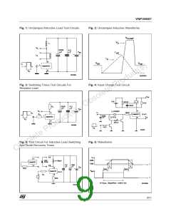
(see figure 3)
td(on)
tr
td(off)
tf
Turn-on Delay Time
Rise Time
Turn-off Delay Time
Fall Time
V
V
DD = 28 V
gen = 10 V
Id = 18 A
Rgen = 1000 Ω
500
2.7
10
800
4.2
16
ns
µs
µs
µs
(see figure 3)
4.3
6.5
(di/dt)on Turn-on Current Slope VDD = 28 V
Vin = 10 V
ID = 18 A
Rgen = 10 Ω
60
A/µs
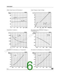
Qi
Total Input Charge
VDD = 12 V ID = 18 A Vin = 10 V
100
nC
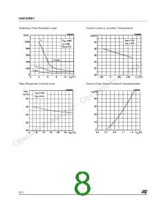
SOURCE DRAIN DIODE
Symbol
Parameter
Test Conditions
Min.
Typ.
Max.
Unit
V
VSD ( ) Forward On Voltage
ISD = 18 A Vin = 0
1.6
trr(
Qrr(
IRRM
)
Reverse Recovery
Time
Reverse Recovery
Charge
Reverse Recovery
Current
I
SD = 18 A
di/dt = 100 A/µs
Tj = 25 C
250
1
ns
o
VDD = 30 V
(see test circuit, figure 5)
)
µC
(
)
8
A
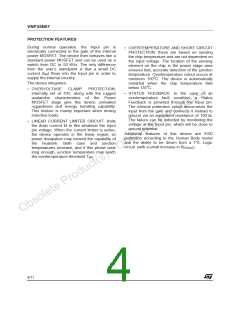
PROTECTION
Symbol
Parameter
Test Conditions
Min.
Typ.
Max.
Unit
Ilim
Drain Current Limit
Vin = 10 V VDS = 13 V
25
25
35
35
45
45
A
A
Vin = 5 V
VDS = 13 V
tdlim
Tjsh
(
(
)
)
Step Response
Current Limit
Vin = 10 V
Vin = 5 V
35
70
60
140
µs
µs
oC
Overtemperature
Shutdown
150
135
Tjrs
(
)
Overtemperature Reset
Fault Sink Current
oC
Igf(
)
Vin = 10 V VDS = 13 V
Vin = 5 V
50
20
mA
mA
VDS = 13 V
o
Eas
(
)
Single Pulse
starting Tj = 25 C
VDD = 20 V
2.5
J
Avalanche Energy
Vin = 10 V Rgen = 1 KΩ L = 10 mH
( ) Pulsed: Pulse duration = 300 µs, duty cycle 1.5 %
) Parameters guaranteed by design/characterization
(
3/11

 STMICROELECTRONICS [ ST ]