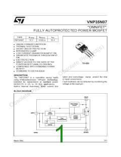
VNP35N07
ABSOLUTE MAXIMUM RATING
Symbol
VDS
Vin
Parameter
Value
Internally Clamped
18
Unit
V
Drain-source Voltage (Vin = 0)
Input Voltage
V
ID
Drain Current
Internally Limited
-50
A
IR
Reverse DC Output Current
Electrostatic Discharge (C= 100 pF, R=1.5 KΩ)
A
Vesd
Ptot
Tj
2000
V
o
Total Dissipation at Tc = 25 C
125
W
oC
oC
oC
Operating Junction Temperature
Case Operating Temperature
Storage Temperature
Internally Limited
Internally Limited
-55 to 150
Tc
Tstg
THERMAL DATA
Rthj-case Thermal Resistance Junction-case
Rthj-amb Thermal Resistance Junction-ambient
Max
Max
1
62.5
oC/W
oC/W
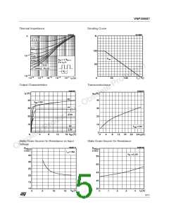
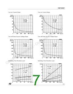
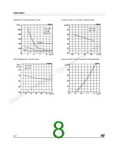
ELECTRICAL CHARACTERISTICS (Tcase = 25 oC unless otherwise specified)
OFF
Symbol
Parameter
Test Conditions
ID = 200 mA Vin = 0
Min.
Typ.
Max.
Unit
VCLAMP Drain-source Clamp
Voltage
60
70
80
V
VCLTH
VINCL
IDSS
Drain-source Clamp
Threshold Voltage
ID = 2 mA Vin = 0
Iin = -1 mA
55
-1
V
V
Input-Source Reverse
Clamp Voltage
-0.3
Zero Input Voltage
Drain Current (Vin = 0) VDS = 25 V Vin = 0
VDS = 13 V Vin = 0
50
200
µA
µA
IISS
Supply Current from
Input Pin
VDS = 0 V Vin = 10 V
250
500
µA
ON ( )
Symbol
Parameter
Test Conditions
VDS = Vin ID + Iin = 1 mA
Min.
Typ.
Max.
Unit
VIN(th)
Input Threshold
Voltage
0.8
3
V
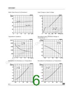
RDS(on)
Static Drain-source On Vin = 10 V ID = 18 A
0.028
0.035
Ω
Ω
Resistance
V
in = 5 V
ID = 18 A
DYNAMIC
Symbol
Parameter
Test Conditions
Min.
Typ.
Max.
Unit
gfs ( )
Forward
VDS = 13 V
ID = 18 A
20
25
S
Transconductance
Coss
Output Capacitance
VDS = 13 V f = 1 MHz Vin = 0
980
1400
pF
2/11

 STMICROELECTRONICS [ ST ]