Pin settings
VIPER16
3
Pin settings
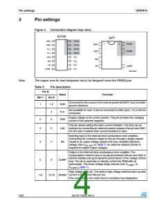
Figure 3.
Connection diagram (top view)
$2!).
$2!).
$2!).
$2!).
$2!).
$2!).
.ꢄ#ꢄ
.ꢄ!ꢄ
!-ꢀꢁꢀꢂꢃVꢁ
Note:
The copper area for heat dissipation has to be designed under the DRAIN pins.
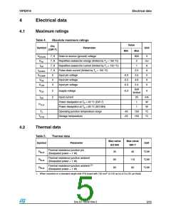
Table 3.
Pin N.
Pin description
Name
Function
DIP-7
SO16
Connected to the source of the internal power MOSFET and controller
ground reference.
1
1-2
GND
N.A.
VDD
Not available for user. It can be connected to GND (pins 1-2) or left not
connected.
-
4
5
Supply voltage of the control section. This pin provides the charging
current of the external capacitor.
2
This pin allows setting the drain current limitation. The limit can be
reduced by connecting an external resistor between this pin and GND.
Pin left open if default drain current limitation is used.
3
4
6
7
LIM
FB
Inverting input of the internal trans conductance error amplifier.
Connecting the converter output to this pin through a single resistor
results in an output voltage equal to the error amplifier reference
voltage (See VFB_REF on Table 7). An external resistors divider is
required for higher output voltages.
Output of the internal trans conductance error amplifier. The
compensation network have to be placed between this pin and GND to
achieve stability and good dynamic performance of the voltage control
loop. The pin is used also to directly control the PWM with an
optocoupler. The linear voltage range extends from VCOMPL to
VCOMPH (Table 7).
5
8
COMP
DRAIN
High voltage drain pin. The built-in high voltage switched start-up bias
current is drawn from this pin too.
7,8
13-16
Pins connected to the metal frame to facilitate heat dissipation.
4/25
Doc ID 15232 Rev 5

 STMICROELECTRONICS [ ST ]