VIPER16
FB pin and COMP pin
12
FB pin and COMP pin
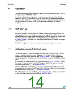
The device can be used both in non-isolated and in isolated topology. In case of non-
isolated topology, the feedback signal from the output voltage is applied directly to the FB
pin as inverting input of the internal error amplifier having the reference voltage, V
REF_FB,
see the Table 8 on page 7.
The output of the error amplifier sources and sinks the current, I
, respectively to and
COMP
from the compensation network connected on the COMP pin. This signal is then compared,
in the PWM comparator, with the signal coming from the SenseFET; the power MOSFET is
switched off when the two values are the same on cycle by cycle basis. See the Figure 2 on
page 3 and the Figure 22 on page 15.
When the power supply output voltage is equal to the error amplifier reference voltage,
V
, a single resistor has to be connected from the output to the FB pin. For higher
REF_FB
output voltages the external resistor divider is needed. If the voltage on FB pin is
accidentally left floating, an internal pull-up protects the controller.
The output of the error amplifier is externally accessible through the COMP pin and it’s used
for the loop compensation: usually an RC network.
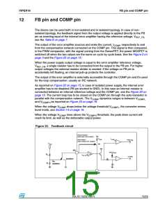
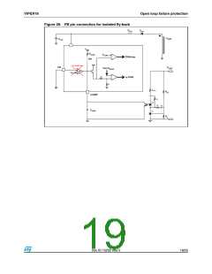
As reported on Figure 22 on page 15, in case of isolated power supply, the internal error
amplifier has to be disabled (FB pin shorted to GND). In this case an internal resistor is
connected between an internal reference voltage and the COMP pin, see the Figure 22 on
page 15. The current loop has to be closed on the COMP pin through the opto-transistor in
parallel with the compensation network. The V
dynamics ranges is between V
COMP
COMPL
and V
as reported on Figure 23 on page 16.
COMPH
When the voltage V
drops below the voltage threshold V
, the converter enters
COMP
COMPL
burst mode, see Section 13 on page 16.
When the voltage V rises above the V
threshold, the peak drain current will
COMPH
COMP
reach its limit, as well as the deliverable output power.
Figure 22. Feedback circuit
Without Isolation:
VREF
switch open & E/A enabled
RCOMP
VCOMPL
With Isolation:
switch closed & E/A disabled
PWM stop
+
-
VOUT
SW
BUS
FB
-
from RSENSE
E/A
+
RH
VREF_FB
to PWM
+
-
nR
Isolation
No
Isolation
RL
R
COMP
Doc ID 15232 Rev 5
15/25

 STMICROELECTRONICS [ ST ]