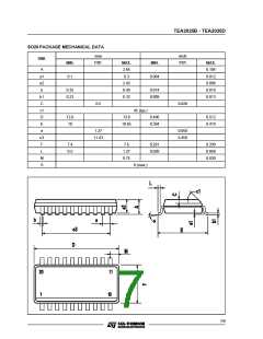
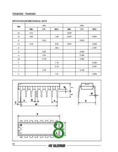
TEA2025B - TEA2025D
The total gain of the bridge is given by:
APPLICATION INFORMATION
Input Capacitor
VOUT
VIN
R1
Rf+R2 +
R3
R4
R1
R2+R4+
=
(1+
)
1
1
Input capacitor is PNP type allowing source to be
referenced to ground.
In this way no input coupling capacitor is required.
However, a series capacitor (0.22 uF)to the input
side can be useful in case of noise due to variable
resistor contact.
JWC1
JWC1
and with the suggestedvalues (C1 = C2 = 100 µF,
Rf= 0) means:
Gv = 52 dB
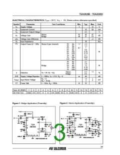
Figure 8
Bootstrap
The bootstrap connection allows to increase the
output swing.
The suggested value for the bootstrap capacitors
(100uF) avoids a reduction of the output signal
also at low frequenciesand low supply voltages.
Voltage Gain Adjust
STEREO MODE
The voltage gain is determined by on-chip resis-
tors R1 and R2 together with the external RfC1
series connected between pin 6 (11) and ground.
The frequency response is given approximated
by:
with first pole at f = 32 Hz
VOUT
VIN
R1
=
Output Capacitors.
The low cut off frequency due to output capacitor
dependingon the load is given by:
1
Rf + R2 +
JWC1
With Rf=0, C1=100 uF, the gain results 46 dB
with pole at f=32Hz.
1
FL =
THE purpose of Rf is to reduce the gain. It is rec-
ommended to not reduce it under 36 dB.
2 ΠCOUT • RL
with COUT 470µF and RL = 4 ohm it means FL =
BRIDGE MODE
Figure 7
80 Hz.
Pop Noise
Most amplifiers similar to TEA 2025B need exter-
nal resistors between DC outputs and ground in
order to optimize the pop on/off performance and
crossoverdistortion.
Figure 9
The bridge configuration is realized very easily
thanks to an internal voltage divider which pro-
vides (at pin 1) the CH 1 output signal after reduc-
tion. It is enough to connect pin 6 (inverting input
of CH 2) with a capacitor to pin 1 and to connect
to ground the pin 7.
The TEA 2025B solution allows to save compo-
nents because of such resistors (800 ohm)are in-
cluded into the chip.
5/9

 STMICROELECTRONICS [ ST ]