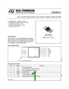
TDA9511
TYPICALAPPLICATION
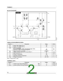
The TDA9511 consists of :
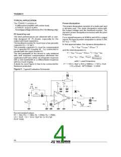
Power dissipation
- A differential amplifier with active load,
- A DMOS output buffer,
- Abandgapvoltagereference(Pin 3forfilteringonly).
The power dissipation consists of a static part and
a dynamic part. The static dissipation varies with
the output voltage and the feedback resistor. The
dynamic power dissipationincreases with the pixel
frequency.
PC board lay-out
The best performances are obtained with a care-
fully designed HF PC-Board, especially for the
output and input capacitors.
ThefeedbackresistorRF must havea low parasitic
capacitor(CF < 0.3pF).
This parasitic capacitor CF must be compensated
by a capacitor R3 (roughly 20 CF) connected in
parallel with the input resistor R1.
The full bandwidth of the device is only obtained
with well matched compensation otherwise the
application will have either an integrator response
with a low bandwidth or a differentiator response
with too much ringing.
For a signalfrequencyof 40MHz and 40VPP output
signal, the typical power dissipation is about 3.0W,
for VDD = 110V.
In first approximation, the dynamic dissipation is :
PD = VDD * CLOAD * ∆VOUT * f
and the total dissipation is :
∆
P = VDD * CLOAD * VOUT * f + VDD * IDD
_____
_____
VOUT
+ VCC * ICC - (VDD - VOUT
)
RFEEDBACK
with f = pixel frequency
A diode DP (see Figure 2) has to be connectedfor
flashoverprotection.
P = 110Vx 10pF x 40V x 40MHz + 110Vx 7mA
+12 x 20mA - 602V/20kΩ = 2.95W
Figure 2 :
Typical Evaluation Schematic
CF
RF
VCC
VDD
IN
R1
DP
2
R3
C3
1
3
7
5
RP
6
CLOAD
VIN
VOUT
4
R2
VOUT
C4
t
Recommended values :
R1 = 1kΩ, R2 = 1.8kΩ, RF = 20kΩ, RP = 200Ω,
C4 > 10nF, C3 = 10 to 12pF for CF # 0.5pF.
R3 # 150Ω.
4/5

 STMICROELECTRONICS [ ST ]