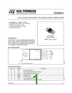
TDA9511
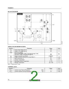
BLOCK DIAGRAM
TDA9511
VDD
7
6
OUT
VCC
IN-
2
1
VREF
AGND
4
5
PGND
3
VREF
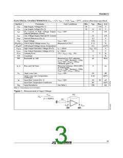
ABSOLUTE MAXIMUM RATINGS
Symbol
Parameter
Value
120
20
Unit
V
VDD
VCC
Supply High Voltage (Pin 7)
Supply Low Voltage (Pin 2)
ESD Susceptibility
V
VESD
Human Body Model, 100pF Discharge through 1.5kΩ
EIAJ Norm, 200pF Discharge through 0Ω
2
300
kV
V
IOD
IOG
Output Current to VDD (Pin 6)
protected
80
Output Current to Ground (Pin 6) (see Note 1)
mA
mA
oC
oC
oC
Ij
Input Current (Pin 1)
50
150
Tj
Junction Temperature
Operating Ambient Temperature
Storage Temperature
Toper
Tstg
0, +70
-20, +150
Note 1 :
≤
µ
Pulsed current t 50 s
THERMAL DATA
Symbol
Parameter
Value
3
Unit
oC/W
oC/W
Rth (j-c)
Rth (j-a)
Junction-Case Thermal Resistance
Max.
Typ.
Junction-Ambient Thermal Resistance
70
2/5

 STMICROELECTRONICS [ ST ]