I2C Bus specification
TDA7719
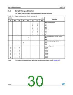
5.2
Data byte specification
The default power on status of the registers is written with underline.
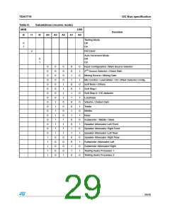
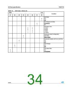
Table 10. Input configuration / main selector (0)
MSB
LSB
D0
Function
D7
D6
D5
D4
D3
D2
D1
Main source selector
0
0
0
0
1
1
1
1
0
0
1
1
0
0
1
1
0
1
0
1
0
1
0
1
IN0
IN1
IN2
IN3
IN4
IN5
IN6
IN7
MD1/2 configuration for main selector
0
1
MD1
MD2
Main source input gain select
0
1
0dB
3dB
Input configuration
CFG0
0
0
0
0
1
1
1
1
0
0
1
1
0
0
1
1
0
1
0
1
0
1
0
1
CFG1
CFG2
CFG3
CFG4
CFG5
CFG6
CFG7
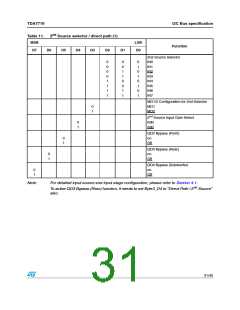
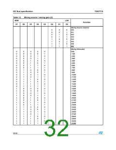
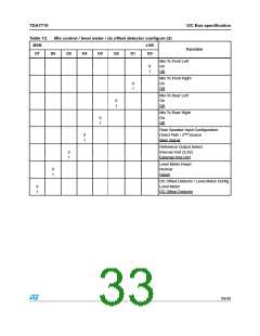
Note:
For detailed input source and input stage configuration, please refer to Section 4.1.
30/45

 STMICROELECTRONICS [ ST ]