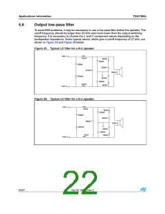
Applications information
TDA7498L
5
Applications information
5.1
Applications circuit
Figure 20. Applications circuit
L4
1
16
17
SUB_GND
OUTPA
OUTPA
C1
22
23
27
INPA
22uH
R15
*
1uF
C2
C3
*
14
15
8R
1nF
PGNDA
PGNDA
S
G
N
D
R6
22R
INNA
C28
C40
C4
1nF
1uF
220nF
J3
S
G
N
D
220nF
SGND
VDDS
DIAG
OUTPUT
C26
680nF
C25
C30
1uF
VDDS
26
C5
J1
*
Load=6 ohm
L+
100nF
12
INPUT
100nF
R1
S
G
N
D
28
*
1
L-
PVCCA
PVCCA
C41
220nF
3 L-
C24
2
100k
13
R-
For
R7
4 L+
1 R-
2 R+
220nF
3
DIAG
C27
J7
22R
Single-Ended
Input
19
R16
8R
R+
VDDPW
PGND
10
4
OUTNA
OUTNA
330pF
S
G
N
D
L3
C6
11
18
25
24
100nF
22uH
2200uF
1
*
VCC
GND
+
C23
IC1
FREQUENCY SHIFT
3
2
SYNCLK
ROSC
GAIN0
GAIN1
SVCC
50V
Q1
1
R13
SYNC
C8
100nF 39K
R3
L1
J2
3
2
2
R9
OUTPB
OUTPB
68Fk S
47k
TDA7498L
22uH
R14
120K
*
R17
8R
S
G
N
D
30
R5
22R
S
G
N
D
J5
J6
S
G
N
D
7
6
C18
220nF
*
PVCCB
PVCCB
VDDS
31
C42
220nF
C19
For
C20
680nF
C31
1uF
*
35
J8
Single-Ended
Input
100nF
C10
100nF
5
4
C43
PGNDB
PGNDB
S
G
N
D
36
32
VSS
C22
220nF
220nF
*
R18
8R
C11
1uF
C12
1uF
INPB
C21
330pF
9
8
OUTNB
OUTNB
3V3
FS
L2
C13
1nF
FS
3
V
3
S
S
S
G
N
D
D
D
33
21
20
INNB
J4
22uH
*
S2
S1
C14
1nF
34
MUTE
1
3
VREF
SVR
R4
C17
G
N
2
MUTE
STBY
+
+
C15
10uF
10V
120k
R2
S
G
N
D
STBY
1
3
2.2uF
G
N
S
G
N
D
29
2
16V
C16
C7
2.2uF
16V
S
S
G
N
D
33k
G
N
D
LC FILTER COMPONENT
10uF
10V
S
G
N
D
S
G
N
D
IN
R8 VCC
6.8k
D1
18V
OUT
1
IC2
L4931CZ33
Load
C20,C26 C18,C22,C24,C28
L1,L2,L3,L4
22 uH
3
C29
TDA7498L
680 nF
470 nF
6 ohm
220 nF
220 nF
C9
GND
2
2.2uF
100nF
S
S
G
N
D
8 ohm
22 uH
S
G
ND
S
G
N
D
G
N
D
S
G
N
D
CLASS-D AMPLIFIER
3V3 POWER SUPPLY
5.2
Mode selection
The three operating modes of the TDA7498L are set by the two inputs, STBY (pin 20) and
MUTE (pin 21).
●
Standby mode: all circuits are turned off, very low current consumption.
●
Mute mode: inputs are connected to ground and the positive and negative PWM
outputs are at 50% duty cycle.
●
Play mode: the amplifiers are active.
18/27
Doc ID 16504 Rev 3

 STMICROELECTRONICS [ ST ]