TDA7377
ELECTRICAL CHARACTERISTICS
Ω
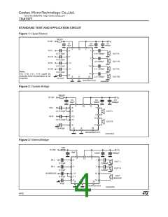
(Referto the test circuit, VS = 14.4V; RL = 4 ; f = 1KHz;
T
amb = 25°C, unless otherwise specified
Symbol
VS
Parameter
Supply Voltage Range
Total Quiescent Drain Current
Output Offset Voltage
Output Power
Test Condition
Min.
Typ.
Max.
Unit
V
8
18
Id
RL = ∞
150
150
mA
mV
VOS
PO
THD = 10%; R = 4
Ω
L
Bridge
18
5.5
20
6
10
W
W
W
Single Ended
Single Ended, R = 2
Ω
L
PO max
PO EIAJ
THD
Max. Output Power (***)
EIAJ Output Power (***)
Distortion
VS = 14.4V, Bridge
VS = 13.7V, Bridge
RL = 4Ω
Single Ended, PO = 0.1 to 4W
Bridge, PO = 0.1 to 10W
31
35
W
W
27
30
0.02
0.03
%
%
0.3
CT
Cross Talk
f = 1KHz Single Ended
f = 10KHz Single Ended
70
60
dB
dB
f = 1KHz Bridge
f = 10KHz Bridge
55
dB
dB
60
RIN
GV
Input Impedance
Voltage Gain
Single Ended
Bridge
20
10
30
15
K
Ω
KΩ
Single Ended
Bridge
19
25
20
26
21
27
dB
dB
GV
EIN
Voltage Gain Match
Input Noise Voltage
0.5
dB
Rg = 0; ”A” weighted, S.E.
Non Inverting Channels
Inverting Channels
2
5
µV
µV
Bridge
Rg = 0; 22Hz to 22KHz
3.5
90
µV
dB
dB
SVR
ASB
ISB
Supply Voltage Rejection
Stand-by Attenuation
Rg = 0; f = 300Hz
PO = 1W
50
80
ST-BY Current Consumption
ST-BY In Threshold Voltage
ST-BY Out Threshold Voltage
ST-BY Pin Current
VST-BY = 0 to 1.5V
100
1.5
A
µ
V
VSB
VSB
Ipin7
3.5
V
Play Mode Vpin7 = 5V
50
5
µA
mA
Max Driving Current Under
Fault (*)
Icd off
Icd on
Clipping Detector
Output Average Current
d = 1% (**)
90
A
µ
Clipping Detector
Output Average Current
d = 5% (**)
160
µA
Vsat pin10
Voltage Saturation on pin 10
Sink Current at Pin 10 = 1mA
0.7
V
(*) See built-in S/C protection description
(**) Pin 10 Pulled-up to 5V with 10KΩ; RL = 4Ω
(***) Saturatedsquare wave output.
3/10

 STMICROELECTRONICS [ ST ]