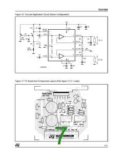
TDA7265
nents are those shown are the demo board sche-
matic different values can be used: the following
table can help the designer.
APPLICATIONS SUGGESTION
(Demo Board Schematic)
The recommended values of the external compo-
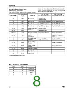
RECOMMENDED
LARGER THAN
RECOMMENDED VALUE RECOMMENDED VALUE
SMALLER THAN
COMPONENTS
PURPOSE
VALUE
Increase of Dz
Biasing Current
R1
10KΩ
Mute Circuit
R2
R3
15KΩ
18KΩ
15KΩ
18KΩ
560Ω
4.7Ω
Mute Circuit
Mute Circuit
Mute Circuit
Vpin # 5 Shifted Downward Vpin # 5 Shifted Upward
Vpin # 5 Shifted Upward
Vpin # 5 Shifted Upward
Increase of Gain
Vpin # 5 Shifted Downward
Vpin # 5 Shifted Downward
R4
R5, R8
R6, R9
R7, R10
Closed Loop Gain
Setting (*)
Decrease of Gain
Frequency Stability Danger of Oscillations
Danger of Oscillations
Input DC
Decoupling
Higher Low Frequency
Cutoff
C1, C2
C3
1µF
1µF
St-By/Mute Time
Larger On/Off Time
Constant
Smaller On/Off Time
Danger of Oscillations
Danger of Oscillations
Supply Voltage
Bypass
C4, C6
C5, C7
1000µF
0.1µF
Supply Voltage
Bypass
C8, C9
Dz
0.1µF
5.1V
Frequency Stability
Mute Circuit
Q1
BC107
Mute Circuit
(*) Closed loop gain has to be => 25dB
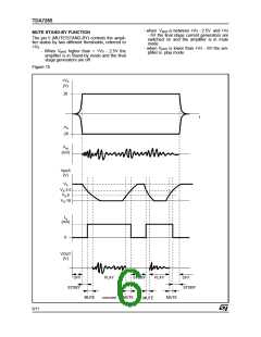
MUTE, STAND-BY TRUTH TABLE
SW1
B
SW2
A
STAND-BY
STAND-BY
MUTE
B
B
A
A
A
B
PLAY
8/11

 STMICROELECTRONICS [ ST ]