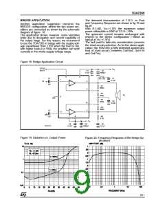
TDA7265
Ω
S
Ω
ELECTRICAL CHARACTERISTICS (Refer to the test circuit, VS = + 20V; RL = 8 ; R = 50 ;
°
GV = 30dB; f = 1KHz; Tamb = 25 C, unless otherwise specified.)
Symbol
Parameter
Supply Range
Test Condition
Min.
Typ.
Max.
Unit
V
VS
Iq
+5
+25
130
+20
Total Quiescent Current
Input Offset Voltage
80
mA
mV
nA
W
VOS
Ib
–20
Non Inverting Input Bias Current
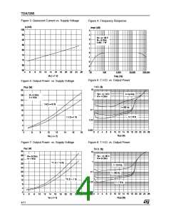
Music Output Power (*)
500
32
PO
THD = 10%; RL = 8Ω ;
VS = + 22.5V
PO
Output Power
THD = 10%
RL = 8Ω ;
VS + 16V; RL = 4Ω
20
25
25
W
W
THD = 1%
RL = 8Ω ;
VS + 16V; RL = 4Ω
20
20
W
W
THD
Total Harmonic Distortion
RL = 8Ω ; PO = 1W; f = 1KHz
0.01
%
%
RL = 8Ω ;
PO = 0.1 to 15W;
f = 100Hz to 15KHz
0.7
1
RL = 4Ω ; PO = 1W; f = 1KHz
0.02
%
%
RL = 4Ω ; VS + 16V;
PO = 0.1 to 12W;
f = 100Hz to 15KHz
CT
Cross Talk
f = 1KHz
f = 10KHz
70
60
dB
dB
SR
GOL
eN
Slew Rate
10
80
V/µs
Open Loop Voltage Gain
Total Input Noise
dB
A Curve
f = 20Hz to 22KHz
3
4
µV
µV
8
Ri
Input Resistance
15
20
60
KΩ
SVR
Supply Voltage Rejection
(each channel)
fr = 100Hz
Vr = 0.5V
dB
Tj
Thermal Shut-down
Junction Temperature
145
°C
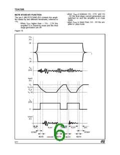
MUTE FUNCTION [ref: +VS]
VTMUTE
AM
Mute / Play Threshold
Mute Attenuation
-7
-6
-5
V
60
70
dB
STAND-BY FUNCTION [ref: +VS]
VTST-BY
AST-BY
Stand-by / Mute Threshold
Stand-by Attenuation
-3.5
-2.5
110
3
-1.5
V
dB
mA
Iq ST-BY
Quiescent Current @ Stand-by
Note :
(*) FULL POWER up to. VS = ±22.5V with RL = 8Ω and VS = ±16V with RL = 4Ω
MUSIC POWER is the maximal power which the amplifier is capable of producing across the rated load resistance (regardless of non linearity)
1 sec after the application of a sinusoidal input signal of frequency 1KHz.
3/11

 STMICROELECTRONICS [ ST ]