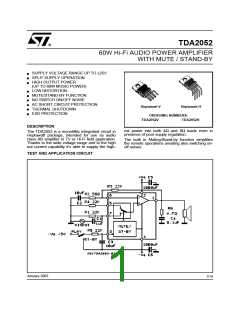
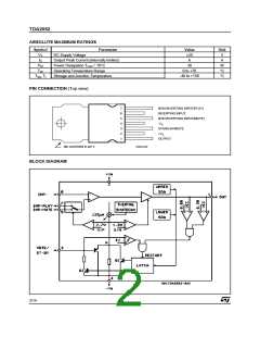
TDA2052
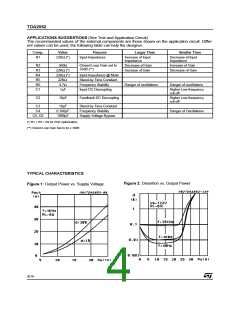
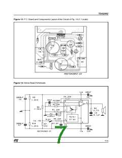
APPLICATIONS SUGGESTIONS (See Test and Application Circuit)
The recommended values of the external components are those shown on the application circuit. Differ-
ent values can be used; the following table can help the designer.
Comp.
Value
Purpose
Larger Than
Smaller Than
R1
22KΩ (*)
Input Impedance
Increase of Input
Impedance
Decrease of Input
Impedance
R2
R3
R4
R5
R6
C1
560Ω
22KΩ (*)
22KΩ (*)
22KΩ
Closed Loop Gain set to
32dB (**)
Decrease of Gain
Increase of Gain
Increase of Gain
Decrease of Gain
Input Impedance @ Mute
Stand-by Time Constant
Frequency Stability
4.7Ω
Danger of oscillations
Danger of oscillations
1µF
Input DC Decoupling
Higher Low-frequency
cut-off
C2
10µF
Feedback DC Decoupling
Higher Low-frequency
cut-off
C3
C4
10µF
Stand-by Time Constant
Frequency Stability
0.100µF
1000µF
Danger of Oscillations
C5, C6
Supply Voltage Bypass
(*) R1 = R3 = R4 for POP optimization
(**) Closed Loop Gain has to be ≥ 30dB
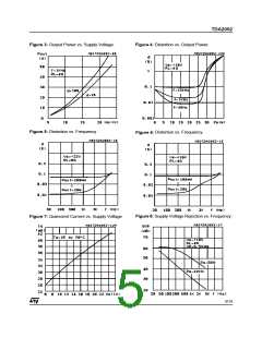
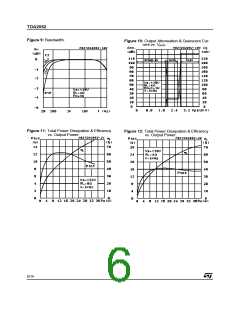
TYPICAL CHARACTERISTICS
Figure 2: Distortion vs. Output Power
Figure 1: Output Power vs. Supply Voltage
4/14

 STMICROELECTRONICS [ ST ]