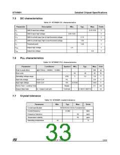
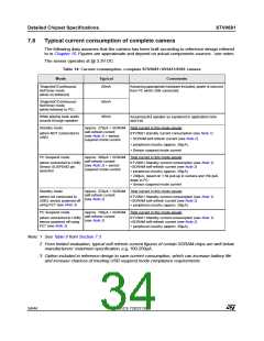
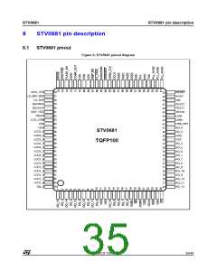
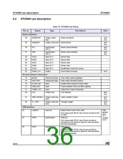
STV0681
STV0681 pin description
Table 15: STV0681 pin listing
Type Description
Pin no.
Signal
drive
RS232 Interface
54
55
TXD
RXD
Output
Serial data transmit
4mA
(SL)
(For camera with USB only, this pin should be tied to
RXD)
Input (S)
Serial data receive
(For camera with USB only, this pin should be tied to
TXD)
STV0680B Master Clocks and Reset
48
49
50
XIN
Input
Quartz Crystal IN
XOUT
RESET
Output
Input (S)
Quartz Crystal OUT
Active (LOW) STV0680B reset
System Memory (SDRAM) Interface
20
22
24
32
34
36
40
41
37
35
33
31
29
30
27
26
DQMU
DCLK
CKE
AD0
Output
Output
Output
Output
Output
Output
Output
Output
Output
Output
Output
Output
Output
Output
Output
Output
Data input/output mask for dram_DQ[15:8]
2mA
(SL)
Clock: all SDRAM input signals are sampled on the
positive edge
4mA
(SL)
Clock enable: activates (HIGH) and deactivates
(LOW) the SDRAM CLK signal
2mA
(SL)
SDRAM address A0
SDRAM address A1
SDRAM address A2
SDRAM address A3
SDRAM address A4
SDRAM address A5
SDRAM address A6
SDRAM address A7
SDRAM address A8
SDRAM address A9
SDRAM address A10
2mA
(SL)
AD1
2mA
(SL)
AD2
2mA
(SL)
AD3
2mA
(SL)
AD4
2mA
(SL)
AD5
2mA
(SL)
AD6
2mA
(SL)
AD7
2mA
(SL)
AD8
2mA
(SL)
AD9
2mA
(SL)
AD10
AD11
AD12
2mA
(SL)
SDRAM address A11 for 64M SDRAM or BA for 16M
SDRAM
2mA
(SL)
SDRAM address A12, BA0 for 64M SDRAM, unused
on 16M
2mA
(SL)
ADCS 7283313C
37/44

 STMICROELECTRONICS [ ST ]