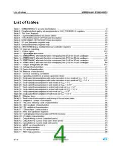
List of tables
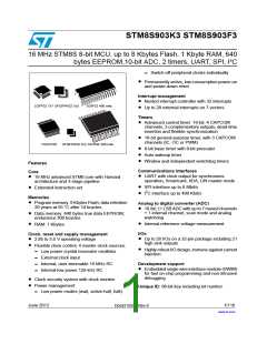
STM8S903K3 STM8S903F3
List of tables
Table 1. STM8S903K3/F3 access line features .......................................................................................9
Table 2. Peripheral clock gating bit assignments in CLK_PCKENR1/2 registers ..................................14
Table 3. TIM timer features ....................................................................................................................16
Table 4. Legend/abbreviations for pinout tables ...................................................................................19
Table 5. TSSOP20/SO20/UFQFPN20 pin description ...........................................................................24
Table 6. UFQFPN32/LQFP32/SDIP32 pin description ...........................................................................24
Table 7. I/O port hardware register map ................................................................................................28
Table 8. General hardware register map ................................................................................................43
Table 9. CPU/SWIM/debug module/interrupt controller registers .........................................................54
Table 10. Interrupt mapping ...................................................................................................................41
Table 11. Option bytes .........................................................................................................................112
Table 12. Option byte description ...........................................................................................................43
Table 13. STM8S903K3 alternate function remapping bits [7:2] for 32-pin packages ...........................45
Table 14. STM8S903F3 alternate function remapping bits [7:2] for 20-pin packages ...........................46
Table 15. STM8S903K3 alternate function remapping bits [1:0] for 32-pin packages .........................102
Table 16. STM8S903F3 alternate function remapping bits [1:0] for 20-pin packages ...........................48
Table 17. Unique ID registers (96 bits) .................................................................................................112
Table 18. Voltage characteristics ...........................................................................................................51
Table 19. Current characteristics ...........................................................................................................51
Table 20. Thermal characteristics ..........................................................................................................52
Table 21. General operating conditions .................................................................................................53
Table 22. Operating conditions at power-up/power-down ......................................................................54
Table 23. Total current consumption with code execution in run mode at VDD = 5 V .............................55
Table 24. Total current consumption with code execution in run mode at VDD = 3.3 V ..........................56
Table 25. Total current consumption in wait mode at VDD = 5 V ............................................................57
Table 26. Total current consumption in wait mode at VDD = 3.3 V .........................................................57
Table 27. Total current consumption in active halt mode at VDD = 5 V ..................................................58
Table 28. Total current consumption in active halt mode at VDD = 3.3 V ...............................................59
Table 29. Total current consumption in halt mode at VDD = 5 V .............................................................60
Table 30. Total current consumption in halt mode at VDD = 3.3 V ..........................................................60
Table 31. Wakeup times .........................................................................................................................60
Table 32. Total current consumption and timing in forced reset state ....................................................61
Table 33. Peripheral current consumption .............................................................................................62
Table 34. HSE user external clock characteristics .................................................................................65
Table 35. HSE oscillator characteristics .................................................................................................65
Table 36. HSI oscillator characteristics ..................................................................................................67
Table 37. LSI oscillator characteristics ...................................................................................................68
Table 38. RAM and hardware registers ..................................................................................................69
Table 39. Flash program memory/data EEPROM memory ....................................................................69
Table 40. I/O static characteristics .........................................................................................................70
Table 41. Output driving current (standard ports) ..................................................................................72
Table 42. Output driving current (true open drain ports) ........................................................................73
Table 43. Output driving current (high sink ports) ..................................................................................73
Table 44. NRST pin characteristics ........................................................................................................78
Table 45. SPI characteristics ..................................................................................................................81
Table 46. I2C characteristics ..................................................................................................................84
Table 47. ADC characteristics ................................................................................................................85
4/116
DocID15590 Rev 8

 STMICROELECTRONICS [ ST ]