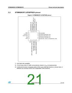
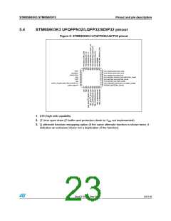
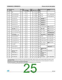
STM8S903K3 STM8S903F3
Pinout and pin description
Input
Output
High
Main
Default alternate function Alternate function after remap
[option bit]
SDIP
32
UFQFPN/ Pin name
LQFP32
Type
function
(after
reset)
floating
wpu Ext.
interrupt
Speed OD
PP
(1)
sink
15
16
17
18
19
20
21
22
23
24
25
26
27
28
29
30
31
32
1
10
11
12
13
14
15
16
17
18
19
20
21
22
23
24
25
26
27
28
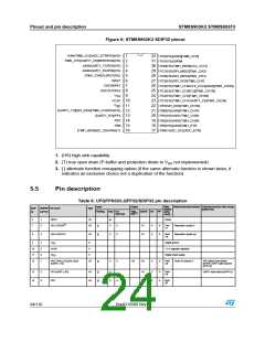
PB6
I/O
I/O
I/O
I/O
I/O
I/O
I/O
I/O
I/O
I/O
I/O
I/O
I/O
I/O
I/O
I/O
I/O
I/O
I/O
X
X
X
X
X
X
X
X
X
X
X
X
X
X
X
X
X
X
X
X
X
O1
O1
O1
O3
O3
O3
O3
O3
O3
O3
O3
O3
O3
O3
O3
O3
O4
O3
O3
X
X
Port
B6
(3)
2
PB5/ I2C_SDA [TIM1_BKIN]
PB4/ I2C_SCL [ADC_ETR]
PB3/ AIN3/TIM1_ETR
PB2/ AIN2/ TIM1_CH3N
PB1/ AIN1/ TIM1_CH2N
PB0/ AIN0/ TIM1_CH1N
PE5/ SPI_NSS [TIM1_CH1N]
X
X
X
X
X
X
X
X
X
X
X
X
X
X
X
X
X
X
T
Port
B5
I
C data
Timer 1 - break input [AFR4]
ADC external trigger [AFR4]
(3)
2
C clock
T
X
X
X
X
X
X
X
X
X
X
X
X
X
X
X
X
Port
B4
I
X
X
X
X
X
X
X
X
X
X
X
X
X
X
X
X
HS
HS
HS
HS
HS
HS
HS
HS
HS
HS
HS
HS
HS
HS
HS
HS
X
X
X
X
X
X
X
X
X
X
X
X
X
X
X
X
Port
B3
Analog input 3/ Timer 1
external trigger
Port
B2
Analog input 2/ Timer 1 -
inverted channel 3
Port
B1
Analog input 1/ Timer 1 -
inverted channel 2
Port
B0
Analog input 0/ Timer 1 -
inverted channel 1
Port
E5
SPI master/ slave select
Timer 1 - inverted channel 1
[AFR1:0]
PC1/ TIM1_CH1/ UART1_CK
[TIM1_CH2N]
Port
C1
Timer 1 - channel 1
UART1 clock
Timer 1 - inverted channel 2
[AFR1:0]
PC2/ TIM1_CH2 [TIM1_CH3N]
Port
C2
Timer 1 - channel 2
Timer 1 - channel 3
Timer 1 - inverted channel 3
[AFR1:0]
PC3/ TIM1_CH3/TLI/[TIM1_CH1N
]
Port
C3
Top level interrupt [AFR3] Timer
1 inverted channel 1 [AFR7]
PC4/ TIM1_CH4/
CLK_CCO/AIN2/[TIM1_CH2N]
Port
C4
Timer 1 - channel 4
/configurable clock output
Analog input 2 [AFR2]Timer 1
inverted channel 2 [AFR7]
PC5/SPI_SCK [TIM5_CH1]
PC6/ SPI_MOSI [TIM1_CH1]
PC7/ SPI_MISO [TIM1_CH2]
PD0/ TIM1_BKIN [CLK_CCO]
Port
C5
SPI clock
Timer 5 channel 1 [AFR0]
Timer 1 channel 1 [AFR0]
Timer 1 channel 2[AFR0]
Port
C6
PI master out/slave in
SPI master in/ slave out
Timer 1 - break input
SWIM data interface
Port
C7
Port
D0
Configurable clock output
[AFR5]
(4)
PD1/ SWIM
Port
D1
PD2/AIN3/ [TIM5_CH3]
Port
D2
Analog input 3 [AFR2] Timer 52
- channel 3 [AFR1]
PD3/ AIN4/ TIM5_CH2/ ADC_ETR
Port
D3
Analog input 4 Timer 52 -
channel 2/ADC external
trigger
2
3
4
5
29
30
31
32
PD4/ TIM5_CH1/ BEEP
[UART1_CK]
I/O
I/O
I/O
I/O
X
X
X
X
X
X
X
X
X
X
X
X
HS
HS
HS
HS
O3
O3
O3
O3
X
X
X
X
X
X
X
X
Port
D4
Timer 5 - channel 1/BEEP
output
UART clock [AFR2]
PD5/ AIN5/ UART1_TX
PD6/ AIN6/ UART1_RX
PD7/ TLI [TIM1_CH4]
Port
D5
Analog input 5/ UART1
data transmit
Port
D6
Analog input 6/ UART1
data receive
Port
D7
Top level interrupt
Timer 1 - channel 4 [AFR6]
(1)
I/O pins used simultaneously for high current source/sink must be uniformly spaced around the package. In addition, the total driven current must respect the absolute maximum ratings ( see section
"Absolute maximum ratings").
(2)
When the MCU is in Halt/Active-halt mode, PA1 is automatically configured in input weak pull-up and cannot be used for waking up the device. In this mode, the output state of PA1 is not driven. It is
recommended to use PA1 only in input mode if Halt/Active-halt is used in the application.
(3)
In the open-drain output column, ‘T’ defines a true open-drain I/O (P-buffer, weak pull-up, and protection diode to V
are not implemented)
DD
(4)
The PD1 pin is in input pull-up during the reset phase and after internal reset release.
DocID15590 Rev 8
25/116

 STMICROELECTRONICS [ ST ]