Product overview
SWIM
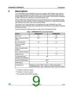
STM8S903K3 STM8S903F3
Single wire interface module for direct access to the debug module and memory programming.
The interface can be activated in all device operation modes. The maximum data transmission
speed is 145 bytes/ms.
Debug module
The non-intrusive debugging module features a performance close to a full-featured emulator.
Beside memory and peripherals, also CPU operation can be monitored in real-time by means
of shadow registers.
R/W to RAM and peripheral registers in real-time
•
R/W access to all resources by stalling the CPU
•
Breakpoints on all program-memory instructions (software breakpoints)
•
Two advanced breakpoints, 23 predefined configurations
•
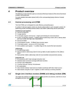
4.3
4.4
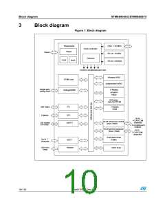
Interrupt controller
Nested interrupts with three software priority levels
•
32 interrupt vectors with hardware priority
•
Up to 28 external interrupts on 7 vectors including TLI
•
Trap and reset interrupts
•
Flash program and data EEPROM memory
8 Kbytes of Flash program single voltage Flash memory
•
640 bytes true data EEPROM
•
User option byte area
•
Write protection (WP)
Write protection of Flash program memory and data EEPROM is provided to avoid unintentional
overwriting of memory that could result from a user software malfunction.
There are two levels of write protection. The first level is known as MASS (memory access
security system). MASS is always enabled and protects the main Flash program memory,
data EEPROM and option bytes.
To perform in-application programming (IAP), this write protection can be removed by writing
a MASS key sequence in a control register. This allows the application to write to data
EEPROM, modify the contents of main program memory or the device option bytes.
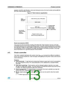
A second level of write protection, can be enabled to further protect a specific area of memory
known as UBC (user boot code). Refer to the figure below.
The size of the UBC is programmable through the UBC option byte, in increments of 1 page
(64-byte block) by programming the UBC option byte in ICP mode.
This divides the program memory into two areas:
Main program memory: Up to 8 Kbytes minus UBC
•
User-specific boot code (UBC): Configurable up to 8 Kbytes
•
The UBC area remains write-protected during in-application programming. This means that
the MASS keys do not unlock the UBC area. It protects the memory used to store the boot
12/116
DocID15590 Rev 8

 STMICROELECTRONICS [ ST ]