STM32F105xx, STM32F107xx
Electrical characteristics
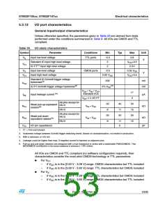
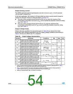
5.3.12
I/O port characteristics
General input/output characteristics
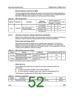
Unless otherwise specified, the parameters given in Table 35 are derived from tests
performed under the conditions summarized in Table 9. All I/Os are CMOS and TTL
compliant.
Table 35. I/O static characteristics
Symbol
Parameter
Input low level voltage
Conditions
Min
Typ
Max
Unit
VIL
TTL ports
–0.5
0.8
V
Standard IO input high level voltage
IO FT(1) input high level voltage
Input low level voltage
2
2
VDD+0.5
5.5V
VIH
VIL
VIH
CMOS ports
–0.5
0.35 VDD
VDD+0.5
V
Input high level voltage
0.65 VDD
Standard IO Schmitt trigger voltage
hysteresis(2)
200
mV
mV
Vhys
IO FT Schmitt trigger voltage hysteresis(2)
5% VDD
(3)
VSS ~ VIN ~ VDD
Standard I/Os
‒1
3
Ilkg
Input leakage current (4)
µA
VIN= 5 V, I/O FT
All pins except for
PA10
30
8
40
11
40
50
15
50
15
Weak pull-up equivalent
resistor(5)
RPU
VIN ?"VSS
kY
PA10
All pins except for
PA10
30
8
Weak pull-down
equivalent resistor(5)
PA10
RPD
VIN ?"VDD
kY
11
5
CIO
I/O pin capacitance
pF
1. FT = Five-volt tolerant.
2. Hysteresis voltage between Schmitt trigger switching levels. Based on characterization, not tested in production.
3. With a minimum of 100 mV.
4. Leakage could be higher than max. if negative current is injected on adjacent pins.
5. Pull-up and pull-down resistors are designed with a true resistance in series with a switchable PMOS/NMOS. This
MOS/NMOS contribution to the series resistance is minimum (~10% order).
All I/Os are CMOS and TTL compliant (no software configuration required), their
characteristics consider the most strict CMOS-technology or TTL parameters:
G
For V :
IH
–
–
if V is in the [2.00 V - 3.08 V] range: CMOS characteristics but TTL included
DD
if V is in the [3.08 V - 3.60 V] range: TTL characteristics but CMOS included
DD
G
For V :
IL
–
–
if V is in the [2.00 V - 2.28 V] range: TTL characteristics but CMOS included
DD
if V is in the [2.28 V - 3.60 V] range: CMOS characteristics but TTL included
DD
Doc ID 15274 Rev 4
53/95

 STMICROELECTRONICS [ ST ]