Electrical characteristics
STM32F105xx, STM32F107xx
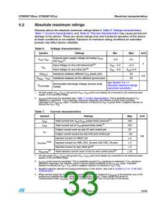
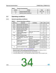
Table 8.
Thermal characteristics
Ratings
Symbol
Value
Unit
TSTG
TJ
Storage temperature range
–65 to +150
150
°C
°C
Maximum junction temperature
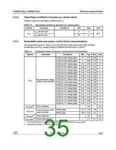
5.3
Operating conditions
5.3.1
General operating conditions
Table 9.
Symbol
General operating conditions
Parameter
Conditions
Min
Max
Unit
fHCLK
fPCLK1
fPCLK2
VDD
Internal AHB clock frequency
Internal APB1 clock frequency
Internal APB2 clock frequency
Standard operating voltage
0
0
0
2
72
36
72
3.6
MHz
V
Analog operating voltage
(ADC not used)
2
3.6
3.6
Must be the same potential
(2)
(1)
VDDA
V
as VDD
Analog operating voltage
(ADC used)
2.4
1.8
VBAT
Backup operating voltage
3.6
V
Power dissipation at TA = 85 °C LQFP100
for suffix 6 or TA = 105 °C for
suffix 7(3)
LQFP64
434
PD
mW
444
Maximum power dissipation
Low power dissipation(4)
–40
–40
–40
–40
–40
–40
85
Ambient temperature for 6
suffix version
°C
°C
°C
105
105
125
105
125
TA
TJ
Maximum power dissipation
Low power dissipation(4)
6 suffix version
Ambient temperature for 7
suffix version
Junction temperature range
7 suffix version
1. When the ADC is used, refer to Table 51: ADC characteristics.
2. It is recommended to power VDD and VDDA from the same source. A maximum difference of 300 mV
between VDD and VDDA can be tolerated during power-up and operation.
3. If TA is lower, higher PD values are allowed as long as TJ does not exceed TJmax.
4. In low power dissipation state, TA can be extended to this range as long as TJ does not exceed TJmax.
34/95
Doc ID 15274 Rev 4

 STMICROELECTRONICS [ ST ]