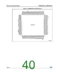
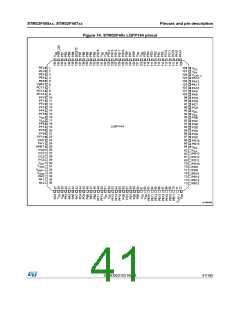
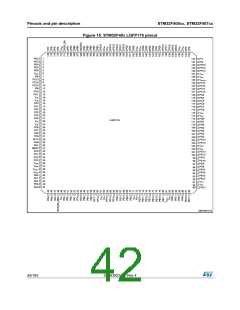
Pinouts and pin description
STM32F405xx, STM32F407xx
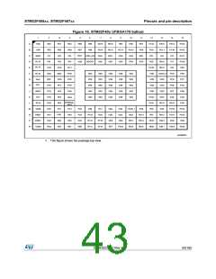
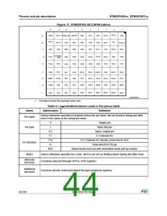
Figure 17. STM32F40x WLCSP90 ballout
10
9
8
7
6
5
4
3
2
1
PA14
A
B
VBAT
PC14
PC13 PDR_ON BOOT0
PB4
PD7
PD4
PC12
VDD
PI1
PC15
VSS
VDD
PB9
PB7
PB6
PB3
PD5
PD6
PD1
PD2
PA15
PI0
VCAP_2
PA11
C
PA0
PC11
PA12
BYPASS_
REG
PA13
VDD
D
PC2
PC0
PB5
VSS
PD0
VDD
PC10
VSS
PA10
PC9
PA9
PC8
PA8
PC7
PB8
VSS
PC3
E
PH1
VDDA
PA3
F
PH0
VDD
PB0
PE10
PE7
PE14 VCAP_1
PC6
PD14
PD12
PD15
PD11
PA1
PA5
G
H
NRST
PE13
PE12
PE15
PB10
PD10
VSSA
PA2
PA6
PA7
PB1
PB2
PE8
PE9
PD9
PD8
PB15
PB13
PE11
PB11
PB12
PB14
J
PA4
MS30402V1
1. This figure shows the package bump view.
Table 6. Legend/abbreviations used in the pinout table
Abbreviation Definition
Name
Unless otherwise specified in brackets below the pin name, the pin function during and after
reset is the same as the actual pin name
Pin name
S
I
Supply pin
Input only pin
Pin type
I/O
FT
TTa
B
Input / output pin
5 V tolerant I/O
3.3 V tolerant I/O directly connected to ADC
Dedicated BOOT0 pin
I/O structure
Notes
RST
Bidirectional reset pin with embedded weak pull-up resistor
Unless otherwise specified by a note, all I/Os are set as floating inputs during and after reset
Functions selected through GPIOx_AFR registers
Alternate
functions
Additional
functions
Functions directly selected/enabled through peripheral registers
44/185
DocID022152 Rev 4

 STMICROELECTRONICS [ ST ]