STM32F405xx, STM32F407xx
Electrical characteristics
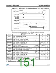
(1)
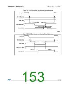
Table 86. Switching characteristics for NAND Flash write cycles
Symbol
Parameter
FSMC_NWE low width
Min
Max
Unit
tw(NWE)
tv(NWE-D)
4THCLK–1
-
4THCLK+ 3
ns
ns
ns
ns
ns
ns
FSMC_NWE low to FSMC_D[15-0] valid
FSMC_NWE high to FSMC_D[15-0] invalid
FSMC_D[15-0] valid before FSMC_NWE high
FSMC_ALE valid before FSMC_NWE low
FSMC_NWE high to FSMC_ALE invalid
0
th(NWE-D)
3THCLK –2
5THCLK–3
-
-
td(D-NWE)
-
td(ALE-NWE)
th(NWE-ALE)
1. CL = 30 pF.
3THCLK
-
3THCLK–2
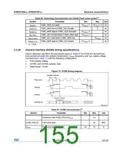
5.3.26
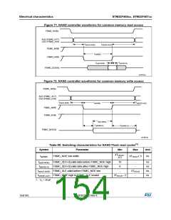
Camera interface (DCMI) timing specifications
Unless otherwise specified, the parameters given in Table 87 for DCMI are derived from
tests performed under the ambient temperature, f frequency and V supply voltage
HCLK
DD
summarized in Table 13, with the following configuration:
•
•
•
PCK polarity: falling
VSYNC and HSYNC polarity: high
Data format: 14 bits
Figure 73. DCMI timing diagram
1/DCMI_PIXCLK
Pixel clock
HSYNC
tsu(HSYNC)
th(HSYNC)
tsu(VSYNC)
th(HSYNC)
VSYNC
tsu(DATA) th(DATA)
DATA[0:13]
MS32414V1
(1)
Table 87. DCMI characteristics
Parameter
Symbol
Min
Max
Unit
Frequency ratio DCMI_PIXCLK/fHCLK
-
0.4
DCMI_PIXCLK
Dpixel
Pixel clock input
-
54
70
MHz
%
Pixel clock input duty cycle
30
DocID022152 Rev 4
155/185

 STMICROELECTRONICS [ ST ]