Electrical characteristics
STM32F405xx, STM32F407xx
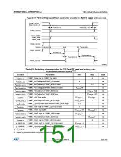
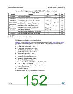
Table 84. Switching characteristics for PC Card/CF read and write cycles
(1)(2)
in I/O space
Parameter
FSMC_NIOWR low width
FSMC_NIOWR low to FSMC_D[15:0] valid
FSMC_NIOWR high to FSMC_D[15:0] invalid
Symbol
Min
Max
Unit
tw(NIOWR)
tv(NIOWR-D)
th(NIOWR-D)
8THCLK –1
-
ns
ns
ns
ns
ns
ns
ns
ns
ns
ns
-
5THCLK– 1
8THCLK– 2
-
td(NCE4_1-NIOWR) FSMC_NCE4_1 low to FSMC_NIOWR valid
th(NCEx-NIOWR) FSMC_NCEx high to FSMC_NIOWR invalid
td(NIORD-NCEx) FSMC_NCEx low to FSMC_NIORD valid
th(NCEx-NIORD) FSMC_NCEx high to FSMC_NIORD) valid
-
5THCLK+ 2.5
5THCLK–1.5
-
-
5THCLK+ 2
5THCLK– 1.5
-
-
tw(NIORD)
tsu(D-NIORD)
td(NIORD-D)
FSMC_NIORD low width
8THCLK–0.5
FSMC_D[15:0] valid before FSMC_NIORD high
FSMC_D[15:0] valid after FSMC_NIORD high
9
0
-
-
1. CL = 30 pF.
2. Based on characterization, not tested in production.
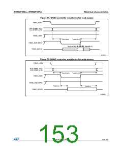
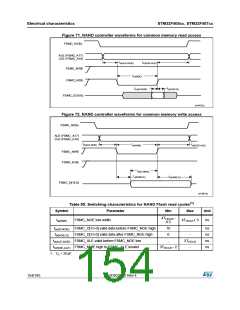
NAND controller waveforms and timings
Figure 69 through Figure 72 represent synchronous waveforms, and Table 85 and Table 86
provide the corresponding timings. The results shown in this table are obtained with the
following FSMC configuration:
•
•
•
•
•
•
•
•
•
•
•
•
•
•
COM.FSMC_SetupTime = 0x01;
COM.FSMC_WaitSetupTime = 0x03;
COM.FSMC_HoldSetupTime = 0x02;
COM.FSMC_HiZSetupTime = 0x01;
ATT.FSMC_SetupTime = 0x01;
ATT.FSMC_WaitSetupTime = 0x03;
ATT.FSMC_HoldSetupTime = 0x02;
ATT.FSMC_HiZSetupTime = 0x01;
Bank = FSMC_Bank_NAND;
MemoryDataWidth = FSMC_MemoryDataWidth_16b;
ECC = FSMC_ECC_Enable;
ECCPageSize = FSMC_ECCPageSize_512Bytes;
TCLRSetupTime = 0;
TARSetupTime = 0.
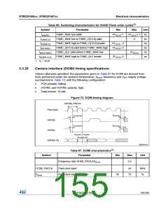
In all timing tables, the THCLK is the HCLK clock period.
152/185
DocID022152 Rev 4

 STMICROELECTRONICS [ ST ]