Electrical characteristics
STM32F302xx/STM32F303xx
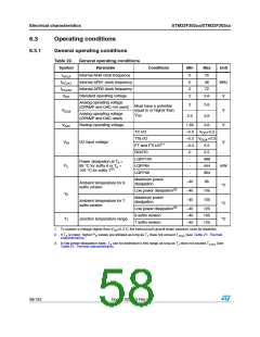
6.2
Absolute maximum ratings
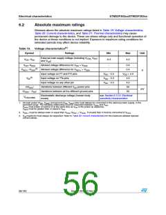
Stresses above the absolute maximum ratings listed in Table 19: Voltage characteristics,
Table 20: Current characteristics, and Table 21: Thermal characteristics may cause
permanent damage to the device. These are stress ratings only and functional operation of
the device at these conditions is not implied. Exposure to maximum rating conditions for
extended periods may affect device reliability.
(1)
Table 19. Voltage characteristics
Symbol
Ratings
Min
Max
Unit
External main supply voltage (including VDDA, VBAT
and VDD
VDD–VSS
-0.3
4.0
)
VDD–VDDA
REF+–VDDA
Allowed voltage difference for VDD > VDDA
Allowed voltage difference for VREF+ > VDDA
Input voltage on FT and FTf pins
-
0.4
0.4
(2)
V
-
V
VSS − 0.3
VDD + 4.0
4.0
(3)
VIN
Input voltage on TTa pins
VSS − 0.3
Input voltage on any other pin
VSS − 0.3
4.0
|ΔVDDx
|
Variations between different VDD power pins
Variations between all the different ground pins
-
-
50
mV
|VSSX − VSS
|
50
Electrostatic discharge voltage (human body
model)
see Section 6.3.12: Electrical
sensitivity characteristics
VESD(HBM)
1. All main power (VDD, VDDA) and ground (VSS, VSSA) pins must always be connected to the external power supply, in the
permitted range. The following relationship must be respected between VDDA and VDD
:
VDDA must power on before or at the same time as VDD in the power up sequence.
V
DDA must be greater than or equal to VDD.
2. VREF+ must be always lower or equal than VDDA (VREF+ ≤ VDDA). If unused then it must be connected to VDDA
.
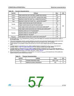
3. VIN maximum must always be respected. Refer to Table 20: Current characteristics for the maximum allowed injected
current values.
56/133
Doc ID 023353 Rev 5

 STMICROELECTRONICS [ ST ]