Electrical characteristics
STM32F302xx/STM32F303xx
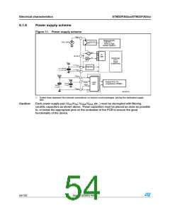
6.1.6
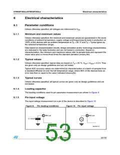
Power supply scheme
Figure 11. Power supply scheme
V
BAT
Backup circuitry
Power switch
(LSE,RTC,
1.65 - 3.6V
Wake-up logic
Backup registers)
OUT
IN
IO
Logic
GP I/Os
Kernel logic
(CPU,
Digital
V
DD
& Memories)
4 ×
3 ×
V
V
DD
Regulator
4 × 100 nF
+ 1 × 4.7 μF
SS
V
DDA
V
DDA
V
REF
!NALOGꢍ 2#Sꢎ 0,,ꢎ
COMPARATORSꢎ /0!- ꢎ ꢏꢏꢏꢏ
V
ADC/
DAC
REF+
10 nF
+ 1 μF
V
REF-
10 nF
+ 1 μF
V
SSA
MS19875V3
1. Dotted lines represent the internal connections on low pin count packages, joining the dedicated supply
pins.
Caution:
Each power supply pair (V /V , V
/V
etc..) must be decoupled with filtering
DD SS
DDA SSA
ceramic capacitors as shown above. These capacitors must be placed as close as possible
to, or below the appropriate pins on the underside of the PCB to ensure the good
functionality of the device.
54/133
Doc ID 023353 Rev 5

 STMICROELECTRONICS [ ST ]