STM32F302xx/STM32F303xx
Electrical characteristics
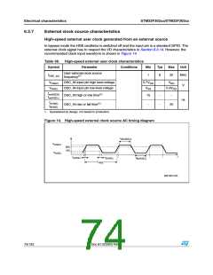
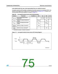
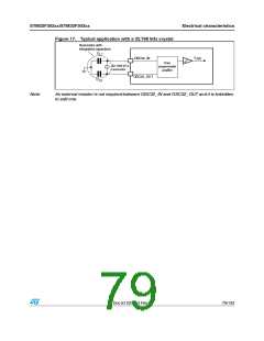
Low-speed external user clock generated from an external source
In bypass mode the LSE oscillator is switched off and the input pin is a standard GPIO. The
external clock signal has to respect the I/O characteristics in Section 6.3.14. However, the
recommended clock input waveform is shown in Figure 15
Table 39. Low-speed external user clock characteristics
Symbol
Parameter
Conditions
Min
Typ
Max
Unit
User External clock source
frequency(1)
fLSE_ext
-
32.768
1000
kHz
OSC32_IN input pin high level
voltage
VLSEH
VLSEL
tw(LSEH)
0.7VDD
VSS
450
-
-
-
-
-
VDD
0.3VDD
-
V
OSC32_IN input pin low level
voltage
OSC32_IN high or low time(1)
OSC32_IN rise or fall time(1)
tw(LSEL)
ns
tr(LSE)
tf(LSE)
50
1. Guaranteed by design, not tested in production.
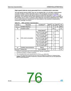
Figure 15. Low-speed external clock source AC timing diagram
T
7ꢐ,3%(ꢑ
6
,3%(
ꢅꢄꢒ
ꢃꢄꢒ
6
,3%,
T
T
T
Rꢐ,3%ꢑ
Fꢐ,3%ꢑ
T
7ꢐ,3%,ꢑ
4
,3%
-3ꢃꢅꢉꢃꢇ6ꢉ
Doc ID 023353 Rev 5
75/133

 STMICROELECTRONICS [ ST ]